PCB warpage is a seemingly small but far-reaching hidden killer in the electronics manufacturing industry. When PCB warpage occurs, it can lead to major problems:
- Poor component contact: A warped PCB makes poor electrical and mechanical contact between components and the PCB, increasing resistance and causing solder joints to overheat.
- Electromagnetic interference: Warped PCBs can create air gaps, reducing the immunity of the circuit to external electromagnetic interference and affecting performance.
- Obstructed mating connections: Warped PCBs may not mate properly with connectors and other mating components, affecting system reliability.
- Obstructed airflow: A severely warped PCB can block cooling airflow, leading to inadequate heat dissipation, which in turn can cause overheating and component failure.
- Physical Damage: Highly warped PCBs are susceptible to damage during assembly or use, resulting in component detachment, solder joints, and fatigue failure of wiring.
- Component Stress: Excessively warped PCBs exert mechanical stress on components, especially BGA and QFN packages, leading to early failure of solder joints.
In this blog, we analyze what causes PCB warpage and what can be done to avoid this costly mistake.
What Causes PCB Warpage?
1.Material and Design Factors
When large PCBs or heavy components are centrally placed, the edge support during reflow soldering can cause the center to sag and form bends.
- V-Cut depth exceeding 1/3 of the board thickness weakens the structural strength, and the difference in CTE between stacked copper (17 ppm/°C) and FR-4 substrate (50-70 ppm/°C) exacerbates the risk of deformation during temperature change.
- Significantly higher copper coverage on one side than the other, with bending effects due to differences in surface tension during cooling.
- Special lamination structures (e.g., asymmetric impedance layer stacking) lead to uncoordinated direction of thermal expansion, resulting in wavy warpage.
- Large-size panels (>400mm) are not designed with reinforcing bars or supporting skeletons, and are prone to center collapse at high temperatures.
- Too many panels in the splicing design, resulting in too many hollow areas, will also weaken the overall rigidity and lead to warpage.
2.Influence of Manufacturing Process
- Excessive temperature fluctuations during pressing of multilayer pcbs, uneven curing of resin to form internal stresses (especially in thicker boards with complex patterns), which are released during subsequent drilling or cutting to trigger deformation.
- Stacking and improper heating during soldermask and silkscreen baking and curing. Causes warpage on both sides of the PCB.
- Differences in CTE between copper foil and glass fiber create residual stress during press-fit, making stress relief more difficult for complex wiring boards.
- Hot Air Solder Leveling (HASL): The entire HASL process is a sudden heating and cooling process. From room temperature to 300 ℃ hot air, then immersed in 265 ℃ tin furnace, and finally rapid water cooling. Inevitably, thermal stresses are generated during the cooling and heating process, leading to the accumulation of micro-strains.
3.Storage and Operation Problems
- Semi-finished products inserted vertically with shelves too tightly spaced, or stacked horizontally with too many layers, PCBs are susceptible to plastic deformation under constant pressure.
- Vibration and improper clamping force in mechanical processing such as depaneling and drilling may induce hidden cracks and expand deformation in subsequent high-temperature processes.
- Failure to bake the PCB before and after cutting it, resulting in internal stresses due to moisture not being removed from the PCB.
How To Prevent PCB Warping and Deformation?
1.Control of Stack Symmetry
Ensure the symmetrical distribution of core board and prepreg, e.g. in a six-layer board, the thickness of layers 1-2 and 5-6, and the amount of prepreg should be exactly the same.
Priority should be given to core boards and prepregs from the same manufacturer to avoid stress imbalance between layers due to material CTE differences.
The area of the outer layer of copper foil should be balanced on both sides. If the copper layer on one side is too small, the balance can be compensated by adding grid copper.
2.Substrate Direction Management
The difference in shrinkage between warp and woof of prepregs should be offset by stacking the layers in the same direction, and the warp direction (direction of copper foil rolling) and the woof direction (long edge of the board) should be strictly aligned.
The long edge of the copper-clad board is usually in the latitudinal direction, so it is necessary to make sure that all prepregs are oriented in the same direction when stacking to avoid anisotropic shrinkage after hot pressing.
3.Mechanical Strength Strengthening
- Large size boards (>400mm) need to be designed with equally spaced reinforcement to avoid center collapse under high temperature.
Reduce the hollow area of the boards, and prioritize the use of honeycomb support structure to improve the overall rigidity.
4.Pre-baking and Dehumidification
- Copper-clad laminates need to be baked at 150℃ for 8±2 hours before cutting to eliminate moisture absorption and expansion stress.
The inner laminates need to be baked twice (4-10 hours) after cutting to ensure that the moisture content of the substrate is <0.1%.
5.Laminating Stress Release
- Cut off or mill burrs immediately after lamination and leave flat in 150℃ oven for 4 hours to fully cure the resin and release residual stresses.
6.Plating Straightening Technology
- 0.4-0.6mm ultra-thin boards need to use special clamping rollers, after clamping the boards on the fly-over of the automatic plating line, automatic straightening is realized through the roller string to prevent deformation caused by high temperature of the plating solution.
7.Hot Air Leveling Cooling Specifications
Some factories in order to improve the brightness of the lead-tin surface. May choose to hot air leveling immediately after the circuit board immersed in cold water cooling. This practice may result in some types of board warpage. The following is the standardized practice:
- Flatten on a marble countertop or steel plate to naturally cool to room temperature.
- An air-float bed cooling system can also be configured to achieve uniform heat dissipation.
8.Reflow Soldering Support Program
- Large-size boards are preferred to adopt long-side feed design, and utilize chains for even weight bearing.
- Use reflow pallet fixtures, if necessary, to provide rigid support for the board body and inhibit thermal cycling deformation.
9.V-Cut alternative process
- Abandon the use of V-cut to separate boards and use router separation instead to avoid loss of structural strength.
Final Thoughts
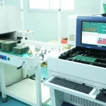
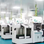
PCB warpage has a direct impact on the reliability and lifespan of electronic devices, and requires precise control at every step of the process, from material selection and process control to storage management. At ApplePCB, we have been specializing in PCB manufacturing for 15 years. By optimizing the stacking design, standardizing the production process, and perfecting the quality inspection system, we can significantly reduce the risk of PCB warpage and ensure that the flatness of each board complies with international standards.
We offer a full range of solutions from design consulting to mass production. For customized PCB manufacturing solutions or technical consulting, please contact ApplePCB's team of engineers.