In electronic designs that prioritize higher power density and reliability, the capacity of thermal management is often a key bottleneck. The low thermal conductivity of traditional FR4 PCBs (0.3 to 0.4 W/mK) often falls short of requirements. Metal-core PCBs (MC/IMS PCBs) address this challenge with their structural design. The metal core efficiently conducts and dissipates heat generated by components, significantly reducing or eliminating the need for additional heat sinks. The thermal conductivity of metal substrates, typically aluminum or copper, ranges from 1 W/mK to 2 W/mK, which is 8 to 9 times greater than that of FR4.
Additionally, there are several notable differences between an MCPCB and an FR4 PCB.
| Features | Metal Core PCB (MCPCB) | FR-4 PCB |
| Heat dissipation mechanism | Metal core directly absorbs heat and quickly conducts and dissipates it. | Relies on through-hole (PTH) and copper layer to conduct heat. |
| PTH (plated through hole) | Not typically available in single-sided boards, surface mount components. | Achievable. |
| Processing (drilling/milling) | Requires diamond-coated saw blade to process metal core. | Standard process. |
| Solder mask | Limited (commonly used in LED applications, such as white). | Various options (green, red, blue, black, etc.) |
| Cost | Typically higher than FR4. | More cost-effective. |
| Rigidity/impact resistance | Excellent (up to 2-4 times that of FR4). | General. |
Key Points in MCPCB Manufacturing
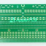
In a typical single-sided LED MCPCB, the circuit layer is bonded with copper foil (1-10 ounces) and heat-conductive dielectric material, and then pressed onto a metal substrate (commonly aluminum 5052/6061 or copper C1100).
| Functions | Functions | Typical thicknesses |
| Metal Substrate | Heat dissipation + mechanical support | 1.0mm/1.5mm/3.2mm(30-125 mils) |
| Dielectric Layer | Electrical isolation + heat conduction (1 to 3 W/mK) | 2-6 mils |
| Conductive pathway | Conductive pathway | 35μm-350μm(1-10oz) |
Metal Substrates in MCPCBs
As the core of heat dissipation, their thickness typically ranges from 30 mils to 125 mils. The most commonly used standard thicknesses include 1.0 mm, 1.5 mm, and 3.2 mm. Metal substrates not only dissipate heat, but also provide structural rigidity to the circuit board, ensuring flatness and making its thickness compatible with standard mounting hardware. Note that the exposed surface of the metal substrate is not coated with any solder mask or surface treatment to maximize its heat dissipation efficiency.
Thermal Conductive Dielectric Layer in MCPCB
The primary function of the thermal conductive dielectric layer (prepreg) is to achieve electrical isolation while facilitating heat transfer. It first absorbs heat generated by electronic components and rapidly dissipates it to the underlying metal substrate.
- Thermal Conductivity: The thermal conductivity coefficient of the dielectric layer is a key metric, typically ranging from 1 W/mK to 3 W/mK. Higher values indicate better heat transfer efficiency.
- Thermal resistance: Reducing the thermal resistance of this layer helps improve overall heat dissipation performance.
- Thickness: Thinner dielectric layers facilitate more efficient heat conduction. The common practical thickness range is 2–6 mils.
- Cost: It is important to note that dielectric materials with higher thermal conductivity typically have higher costs.
Plated-through Holes in MCPCBs
When designing MCPCBs, an important principle is to minimize or avoid the use of plated-through holes (PTH) that penetrate the metal substrate, and instead prioritize surface mount technology (SMT) components. This is because the metal substrate is conductive, and if through-hole components are directly drilled and installed, their pins will come into contact with the metal substrate, causing a short circuit.
Solutions When PTHs Are Necessary:
- Enlarged holes: Drill a hole in the metal substrate at the required PTH location that is 40 mils (approximately 1 mm) to 50 mils (approximately 1.27 mm) larger than the final required hole diameter.
- Insulation filling: Completely fill and cure the enlarged hole with non-conductive epoxy resin filler.
Manufacturing of Multi-Layer MCPCBs
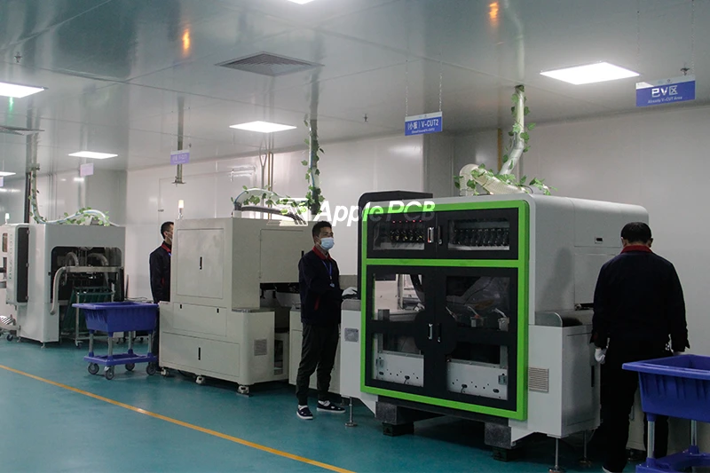
- Lamination Sequence: After the metal substrate has undergone necessary via hole area insulation filling and surface cleaning, it can be laminated together with other inner layer core materials.
- PTH Drilling: After lamination is complete, the required plated-through-hole (PTH) drilling and plating are performed.
- Process Simplification Advantages: Unlike conventional FR4 LED PCBs, MCPCBs rely on the metal substrate itself for heat dissipation, eliminating the need for densely designed thermal vias beneath components. This significantly reduces drilling workload and simplifies the manufacturing process.
- Single-sided PCB process differences: For single-sided MCPCBs, due to their simple structure and lack of via requirements, the chemical copper plating (chemical electroplating) step can be skipped, and circuit pattern transfer (imaging) can be performed directly. Subsequent processes such as etching, solder mask application, character printing, and surface treatment are similar to those in standard FR4 PCB manufacturing.
Laminate Requirements In MCPCBs
When constructing multi-layer metal core PCBs, in order to minimize board warping and deformation, the laminate structure on both sides of the metal substrate must be symmetrical. This means:
- Symmetrical layer count: The number of copper layers on the top of the metal substrate should be equal to the number of copper layers on the bottom.
- Symmetrical copper thickness: If copper foils of different thicknesses are used, they should also be distributed symmetrically on both sides of the metal core (similar to the requirement for symmetrical copper distribution in conventional multilayer PCBs).
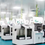
Advances in MCPCB Manufacturing Technology
As modern electronic products demand higher performance, MCPCB manufacturing technology has undergone rapid innovation. Next, we will discuss several notable technologies that have emerged in recent years.
1.Laser Direct Structuring (LDS) Technology
When it comes to MCPCB innovation, Laser Direct Structuring (LDS) is undoubtedly a game-changing technology. By using lasers to create precise circuit patterns directly on the surface of the substrate, this technology offers several significant advantages:
- High precision: LDS technology can produce small and complex circuit patterns with high precision.
- Flexibility: LDS technology does not require additional tool changes, allowing for quick adjustments and modifications to circuit designs.
- Cost reduction: By reducing multiple production steps and tool changes, LDS effectively lowers production costs and accelerates the manufacturing process.
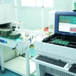
2.Automated Inspection Technology (AOI and AXI)
There have also been significant innovations in automated inspection technology. In particular, automated optical inspection (AOI) and automated X-ray inspection (AXI) systems have significantly improved the quality assurance of MCPCBs.
- Defect Detection: These automated systems can detect defects that are difficult to identify through traditional manual inspections, such as misalignment, cracks, and voids, ensuring flawless product quality.
- Improved Efficiency: Automation reduces the time and labor required for manual inspections, making production more efficient.
- Reliability: Automated inspection systems provide stable and precise results, reducing human error and enhancing reliability.
3.Advanced Laminating Technology
- High-Pressure Laminating: By applying higher pressure, the interlayer bonding strength is enhanced, improving the mechanical strength and reliability of the board.
- Vacuum Laminating: This process eliminates bubbles and voids within the dielectric layer, thereby enhancing thermal conductivity and electrical stability.
Wrapping Up
In this article, we explored the characteristics of metal-core PCBs and the key points of their fabrication from the perspective of a PCB manufacturer. With 16 years of experience in metal-core PCB manufacturing, ApplePCB is committed to staying up to date and encouraging our engineers and technical teams to keep pace with technological advancements. If you have any questions about MCPCB manufacturing, our team is ready to provide professional assistance.