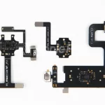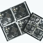
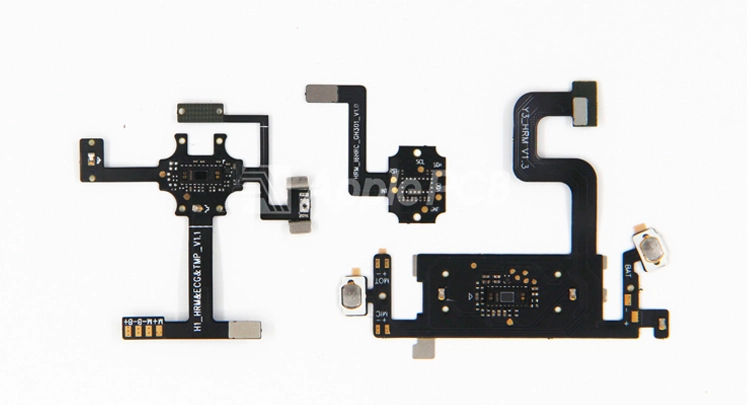
In PCB fabrication, flexible PCBs present a significantly higher level of process complexity than conventional rigid PCB. Beyond establishing precise fine-line copper interconnections, flex fabricators must guarantee long-term electrical reliability and dynamic mechanical durability under continuous bending, twisting, and flexing cycles. From substrate selection to micro-machining process control, every fabrication phase requires specialized handling.
Despite these unique requirements, the core engineering logic of flex PCB fabrication shares foundational principles with standard rigid PCB processing. Many primary manufacturing stages are conceptually parallel; the fundamental differences stem from flexible polymer material chemistries, coverlay lamination techniques, and specialized handling controls designed to maximize flexural fatigue resistance.
This guide breaks down the 7 core process steps in flexible PCB fabrication, detailing the complete manufacturing workflow from raw material preparation through final inspection and shipment.
Step 1: FCCL Fabrication
Flexible PCB manufacturing begins with substrate preparation, centered on the fabrication of FCCL. Unlike rigid PCBs that utilize glass-reinforced epoxy, FPC base substrates consist of a composite stackup incorporating copper foil, PI film, and specialized adhesives.
During initial material preparation, fabricators select either RA copper foil or ED copper foil based on application requirements, alongside high-performance PI films and bonding adhesives. Copper foil undergoes precision cold rolling to achieve the design target thickness. Simultaneously, an adhesive coating is applied to the PI film matrix before being continuously laminated with the copper foil under controlled high-temperature, high-pressure hydraulic cycles, yielding a structurally uniform FCCL substrate. The PI coverlay film integrated during these early processing phases serves a protective role equivalent to solder mask on rigid boards.
In standard volume production, PI base films are available in standard dielectric thicknesses of 12.5 µm, 25 µm, 50 µm, and 75 µm. Copper foil options typically span 12 µm, 18 µm, 35 µm, and 70 µm, with bonding adhesive layers applied at a nominal 20 µm thickness. The specific ratio of dielectric to copper thickness dictates the finished FPC dynamic flexural fatigue life, minimum bend radius, and controlled impedance parameters.
Once FCCL panel preparation is complete, the substrate advances to drilling and photolithographic circuit pattern formation.
Step 2: Laser Via Drilling
Following FCCL panel preparation, conductive vias must be formed at targeted pad locations to enable vertical interconnects between layers. Depending on via diameters and throughput demands, FPC fabrication deploys three primary drilling methodologies: mechanical drilling, laser microvia ablation, and mechanical punching.
- Mechanical CNC Drilling for Through-Holes
For larger through-hole geometries and conventional via diameters, mechanical CNC drilling remains the primary choice. In high-volume roll-to-roll production, multiple flex substrate webs are stacked and fed into multi-spindle drilling machines simultaneously. The layered web stack undergoes synchronized drilling before being rewound onto individual take-up reels at the machine exit, dramatically increasing throughput. For panel-based FPC fabrication, sheets are clamped between rigid entry and backing boards during drilling. This panelized approach demands strict registration control, as mechanical alignment precision on flexible substrates is inherently lower than on rigid boards.
- Laser Ablation for Microvias
When via diameters shrink down to micro-scale dimensions, fabricators deploy laser microvia drilling. UV lasers and YAG lasers deliver superior optical beam precision for sub-100 µm microvias. For mid-range via diameters of 4 mils and above, CO₂ lasers are implemented for rapid ablation. Laser drilling incurs higher operational costs and requires single-sheet panel processing, yielding lower panel-per-hour output than multi-spindle mechanical drilling.
- Mechanical Punching & Slotting
For oversized clearance holes and non-circular cutout slots, specialized punch-die tooling is utilized. Because mechanical punching operates as a standalone fabrication step, it is handled separately from main panel drilling operations.
Once drilling and hole quality inspection are complete, the drilled FCCL panel advances to desmear, hole-wall metallization, and photolithographic circuit patterning.
Step 3: Hole Metallization
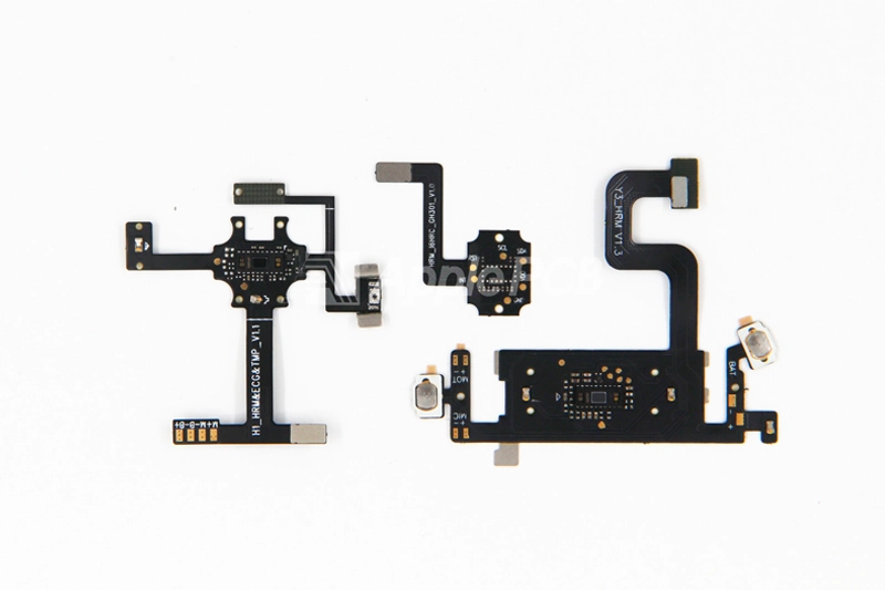
Following drilling, conductive copper must be deposited onto non-conductive via hole walls to establish vertical interconnections. The underlying chemistry mirrors standard rigid PCB Plated Through-Hole processing: an electroless copper deposition step first establishes a thin conductive seed layer on the PI hole wall, followed by electrolytic copper plating to build up final barrel thickness.
Flex PCBs impose stricter minimum hole-wall copper plating standards than rigid boards. To ensure via barrels and land pads withstand mechanical strain during continuous dynamic flex cycles, hole-wall plating thickness is maintained at a minimum of 1 mil (25 µm). By comparison, standard rigid PCBs often accept nominal 0.5 mil hole-wall plating. This additional copper mass is critical—thinner via barrels are highly susceptible to fatigue cracking under repeat mechanical stress, resulting in open-circuit failures.
FastlinkPCB utilizes Vertical Continuous Plating lines for FPC hole metallization. VCP technology optimizes current density distribution across the panel, delivering uniform copper plating distribution down high-aspect-ratio vias and ensuring consistent mechanical integrity throughout the entire production array.
Once hole metallization and surface copper build-up are complete, panels advance to dry-film photolithography and fine-line pattern etching.
Step 4: Photolithography & Etching
With hole metallization complete, the next objective is transferring circuit layout geometries onto the outer copper foil. This photolithographic pattern transfer mirrors rigid PCB techniques, though flexible polymer handling demands tighter process controls to prevent substrate dimensional distortion.
- Photoresist Application: A liquid or dry film photosensitive photoresist layer is uniformly laminated onto the copper foil.
- UV Exposure & Development: Using target Gerber layer data, UV exposure tools project high-resolution circuit patterns onto the photoresist. Photons induce cross-linking polymerization in exposed regions, rendering them insoluble. Panels undergo alkaline chemical development to wash away unexposed photoresist, revealing bare copper while leaving cured photoresist over designed trace geometries.
- Subtractive Chemical Etching: Panels enter chemical spray chambers where acidic or basic etchants (such as cupric chloride or ferric chloride solutions) dissolve bare, unprotected copper. Cured photoresist shields the underlying copper tracks. Stripping solutions then remove the remaining photoresist mask, leaving distinct conductor traces and pad features.
Subtractive fine-line photolithography serves as a cornerstone of FPC fabrication, directly governing routing density and conductor pitch. Leveraging stable polymer backings and direct imaging photolithography, flex substrates achieve fine-line interconnections. In high-volume production, maximum pad-to-trace pitch scales down to 0.35 mm, with standard minimum line width/space metrics rated at 0.15 mm / 0.15 mm (6 mil / 6 mil) and a trace width tolerance held within ±0.05 mm.
Step 5: Polyimide Coverlay
Following circuit etching and stripping, exposed copper conductors require insulation and mechanical protection against oxidation, environmental moisture, and handling damage. In FPC fabrication, this protective barrier is established using a polyimide coverlay or liquid solder mask, performing a function equivalent to liquid photoimageable solder mask on rigid PCBs.
Fabricators execute coverlay protection via two primary process pathways:
- Pre-Punched Polyimide Coverlay Lamination
Laminated PI coverlay film represents the standard protective method for flexible circuits. Composed of a PI film backing coated with a specialized acrylic or epoxy adhesive layer, the coverlay is pre-cut or CNC punch-routed to create window openings matching component solder pads. The aligned coverlay sheet is then permanently bonded to the circuit surface using high-temperature vacuum hydraulic press cycles. This mature process delivers superior mechanical flexibility and dielectric strength.
- Photoimageable Liquid Solder Mask & Screen Printing
For high-density FPCs with complex pad configurations, photoimageable liquid coverlay is applied directly across the panel surface. Access windows over solder pads are formed via optical UV exposure and liquid chemical development, followed by full UV or thermal curing. This method eliminates die-cutting setup steps, making it ideal for fine-pitch SMT pads. On budget-sensitive or low-density flex designs, coverlay coatings can also be applied via screen printing and UV thermal curing.
Key Engineering Distinction: Solid PI coverlay film is laminated as a pre-formed sheet under vacuum heat, whereas liquid coverlay is applied as a wet polymer and chemically cured into a solid film.
Step 6: Flexible PCB Routing
Once coverlay lamination and curing are complete, the flexible circuit geometry is fully defined. The panel then advances to final profiling—a process commonly referred to as blanking, punching, or singulation—to separate individual FPCs from the working production panel.
Depending on production volume, ApplePCB utilizes two primary profiling methodologies:
- Hard Tooling & Hydraulic Blanking Dies
For high-volume production runs, fabricators deploy precision hydraulic blanking presses fitted with hardened steel die sets. While hard tooling requires higher upfront engineering and tooling costs, a single hydraulic press stroke punches multiple flex circuits simultaneously. This minimizes per-unit processing time and drastically reduces unit fabrication costs over extended production runs.
- Steel Rule Dies for Low-Volume & Prototyping
For prototype builds and low-volume orders, fabricators utilize steel rule dies to cut panel outlines. A steel rule die consists of pre-bent razor-sharp steel blades fitted into CNC-milled slots within a rigid baseboard (such as high-density fiberboard, hardwood plywood, or dense synthetic substrate). Manual or semi-automatic mechanical pressing forces the flex panel against the steel blades to trim the board perimeter. This approach avoids expensive hard tooling setups, offering a cost-effective profiling solution for short runs.
Following profile blanking, individual flex circuits proceed to final electrical testing, automated optical inspection, and quality assurance.
Step 7: Rigid-Flex Lamination
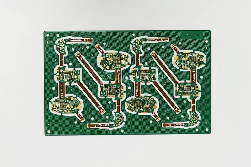
When flexible circuits must integrate with rigid board sections to form rigid-flex PCBs, the processed flex cores—having completed coverlay lamination and preliminary outline routing—advance to rigid-flex multilayer lamination. This step serves as a critical bridge integrating dynamic flexible interconnects with structural rigid sub-assemblies.
During layer layup, flex circuit cores are precisely registered between rigid FR-4 panels. Non-bonded flexible tail sections temporarily attach to sacrificial FR-4 or MDF carrier backing plates to guarantee dimensional alignment during press loading. The complete composite stackup undergoes high-temperature, high-pressure vacuum lamination. Specialized structural adhesives (such as acrylic or no-flow epoxy adhesive films) and low-flow rigid prepregs permanently bond the flexible tails and rigid cores into a unified substrate.
Stackup Design Guidelines for Flexible Arms
- Adjacent Flex Layers: In multi-layer flex-rigid stackups, adjacent flexible circuit layers can be laminated directly together or separated using thin PI bonding sheets and no-flow prepregs.
- Copper Layer Threshold: To preserve dynamic flexural fatigue resistance, individual unbonded flex arms are restricted to a maximum of 2 copper layers (1 oz or 1/2 oz copper). Exceeding 2 copper layers in a flexible bending zone drastically reduces dynamic bend life and increases micro-fracture risks.
Once vacuum lamination cycles are complete, rigid panel zones retain exposed flexible interconnect arms engineered specifically for tight-radius dynamic or flex-to-install applications. The panelized rigid sections then advance to secondary CNC drilling, PTH hole metallization, and outer-layer circuit photolithography to finalize the complete rigid-flex structure.
Final Thoughts
The 7 core process stages detailed above form the foundation of high-reliability flexible circuit board manufacturing. To optimize yield rates, lower production costs, and ensure long-term dynamic flex reliability, consider these key DFM guidelines when planning your FPC or rigid-flex project:
- Material Stackup
The thickness ratio between the PI dielectric substrate and copper foil directly governs the minimum bend radius and dynamic flexural fatigue life. For applications requiring high-cycle dynamic bending, consult with your fabricator during early layout to select optimal combination ratios (such as 1/2 oz RA copper paired with 12.5 µm PI film).
- Fine-Line Trace & Space Optimization
While advanced photolithography can resolve fine line geometries down to 50 µm (2 mil), ultra-tight conductor spacing increases fabrication complexity and impacts overall panel yield. Incorporating realistic design margins rather than pushing minimum process limits delivers superior cost-efficiency during volume production.
- Rigid-Flex Transition Zone
Flex Layer Count: Restrict unbonded flexible arms to a maximum of 2 copper layers. Exceeding 2 copper layers drastically degrades flexural performance and increases mechanical stress fatigue.
Transition Relief: Ensure adequate strain relief clearance at the interface where the flexible tail emerges from the rigid substrate to prevent stress concentrations and copper trace fractures.
Because fabrication capabilities and tolerance windows vary across production facilities, executing early DFM evaluations with your manufacturing team remains the most effective strategy. Resolving stackup, impedance, and bend-radius challenges during Gerber layout is vastly more efficient than troubleshooting physical yield failures post-fabrication.
If you are developing a new FPC or rigid-flex hardware design, contact ApplePCB's engineering team today to receive complete DFM reviews, stackup optimization, and technical support from prototype through volume delivery.