Compared to traditional FR-4, Aluminum Core PCBs (also known as Metal Core PCBs or MCPCBs) leverage the high thermal conductivity of an integrated metallic substrate to rapidly pull heat away from high-power surface-mount components.
However, taking an aluminum PCB project from raw Gerber files to a fully qualified, high-reliability finished board involves processing techniques and engineering considerations that differ drastically from standard fiberglass manufacturing. In this technical walkthrough, we take an inside look at the step-by-step fabrication sequence of aluminum core PCBs from the perspective of the factory floor.
1.Thermal Design & Layout Optimization
During the layout phase of an aluminum board, engineers must prioritize thermal management alongside basic electrical routing.
- Trace Width & Clearance Optimization: Aluminum core PCBs typically drive high-power, high-current circuits. To handle high amperage without localized I²R heating or dielectric breakdown, trace widths and safety clearances must be sized generously based on copper weight—typically starting at 1 oz and scaling up to 2 oz or 3 oz heavy copper.
- Thermal Path Planning: High-wattage active devices should be spatially distributed across the layout to prevent localized thermal hotspots. Additionally, large copper thermal pads should be flooded directly beneath power components to maximize the contact area transferring heat into the dielectric layer and aluminum base below.
- Minimizing Plated Vias: In standard multi-layer FR-4 designs, through-vias are routine for routing between layers. In single-sided MCPCBs, however, drilling through the metal base compromises electrical isolation and requires complex insulated-sleeve processes. Unless specifying a specialized dual-sided or blind-via MCPCB stackup, designs should eliminate unnecessary via holes altogether.
Pre-Flight DFM Review
Once layout design is complete, files are exported as standard Gerber packages (covering trace layer, solder mask, legend, and mechanical outline). Before releasing job tickets to the factory floor, engineering teams run a strict Design for Manufacturability (DFM) audit. This step verifies trace geometry, copper clearance to board edge, and thermal dissipation paths—catching potential fabrication hazards before raw material is processed.
2.Material Selection & Substrate Architecture
Upward of 80% of an aluminum board’s thermal and mechanical performance comes down to raw material selection. An aluminum PCB comprises a three-layer stackup: a Copper Circuit Layer, a Thermally Conductive Dielectric Layer, and a Base Aluminum Substrate.
The specific aluminum alloy grade and the thermal conductivity rating of the bonding dielectric dictate the thermal dissipation limit, dielectric breakdown voltage, and overall structural rigidity.
Primary Aluminum Alloy Grades
Depending on operating environments and mechanical stress profiles, manufacturers utilize three primary aluminum alloys for the metallic base:
- 5052 Aluminum Alloy: The industry workhorse for general-purpose MCPCBs. 5052 offers superior corrosion resistance, high formability, and reliable moderate structural strength—making it ideal for high-volume commercial LED fixtures and power supplies.
- 6061 Aluminum Alloy: Delivering excellent thermal conductivity, high hardness, and superior CNC machinability. 6061 is preferred for high-stress automotive control modules, power electronics, and industrial systems requiring tight-tolerance milling or direct mechanical mounting.
- 7075 Aluminum Alloy: Offering exceptionally high yield strength and extreme fatigue resistance. While more costly and harder to process, 7075 is reserved for aerospace electronics, military hardware, and extreme heavy-duty mechanical environments.
Base Substrate Thickness Considerations
Standard aluminum backing thickness ranges from 1.0 mm up to 6.0 mm, depending on two key operational parameters:
- Mechanical Structural Integration: Whether the board serves as a load-bearing chassis component bolted directly to external heat exchangers or housings.
- Transient Thermal Mass: Thicker metal backing provides a larger thermal buffer, absorbing sudden spikes in thermal energy during burst power operation.
Fabrication Capability Limits
Machining aluminum substrates demands heavy-duty tooling to avoid material deformation. Manufacturing capabilities support substrate thickness options from 1.0 mm to 6.0 mm. Utilizing specialized tungsten carbide V-scoring units and high-torque CNC routers ensures clean, burr-free mechanical edges without causing micro-delamination between the thin dielectric layer and the aluminum base.
3.Surface Pre-Treatment & Micro-Texturing
Prior to laminating the raw aluminum backing with the thermally conductive dielectric layer and top copper foil, the surface of the metal base must undergo rigorous chemical and physical preparation. The microscopic cleanliness and surface energy of the aluminum face dictate overall peel strength. Without precise surface pre-treatment, an aluminum PCB will suffer from delamination (layer separation) when exposed to high-temperature reflow soldering (260℃) or long-term operational thermal cycling.
Crucial Surface Preparation Steps
- Chemical Degreasing: Cold-rolled aluminum stock carries residual cutting oils, lubricants, and anti-corrosion films from raw material processing. Boards pass through alkaline degreasing baths to strip away all organic films and particulate contaminants.
- Oxide Removal & Acid Pickling: Raw aluminum rapidly forms a native, non-uniform aluminum oxide passivation film when exposed to ambient air. Because this loose oxide layer compromises mechanical adhesion, acid pickling and micro-etching are used to strip away the native film, exposing a fresh, reactive aluminum metal matrix.
- Mechanical Micro-Texturing: Smooth aluminum provides insufficient mechanical lock for bonding resins. Using controlled chemical micro-etching or high-pressure micro-sandblasting, the metallic surface is textured with a uniform microscopic anchor profile. This microscopic roughness dramatically increases interfacial bond strength and shear resistance.
Preventing Secondary Oxidation
Exposed aluminum oxidizes in seconds when exposed to ambient moisture. Factory process controls enforce tight time-window limits between surface pickling, thermal drying, and vacuum lamination. Utilizing automated conveyorized wash lines and dust-free drying tunnels ensures uniform surface anchor profiles across every panel, eliminating delamination risk at the source.
4.Lamination & Composite Bonding
Once surface pre-treatment is complete, the high-conductivity copper foil must be permanently bonded to the aluminum backing plate via the insulating dielectric interlayer.
- Stackup Registration: High-purity Oxygen-Free High Thermal Conductivity (OFHC) copper foil, the pre-impregnated thermal dielectric sheet, and the prepared aluminum base plate are stacked in precise mechanical registration.
- Vacuum Hot-Press Lamination: The stacked panel assemblies are transferred into a multi-stage vacuum hot press. Controlled high-temperature profiles and high hydraulic pressure drive out trapped air, preventing micro-void formation.
- Interfacial Bonding & Resin Curing: Under controlled pressure and heat, the thermal polymer dielectric undergoes cross-linking and thermoset curing. Micro-diffusion across the material boundaries creates an ultra-strong mechanical and chemical bond with exceptional peel strength.
Quality Validation & Thermal Stress TestingInterfacial adhesion strength is verified through rigorous destruct-testing protocols. Samples from every press batch undergo two primary quality assurance checks:
- Peel Strength Test: Quantifies the force ($N/\text{mm}$) required to strip the bonded copper trace away from the dielectric substrate.
- 288℃ Solder Float Test: Submerges the laminated sample in a molten solder bath at 288℃for 10 seconds. This severe thermal shock verifies that the dielectric and copper layers will not blister, delaminate, or warp during automated SMT reflow assembly.
5.Imaging, Photolithography & Chemical Etching
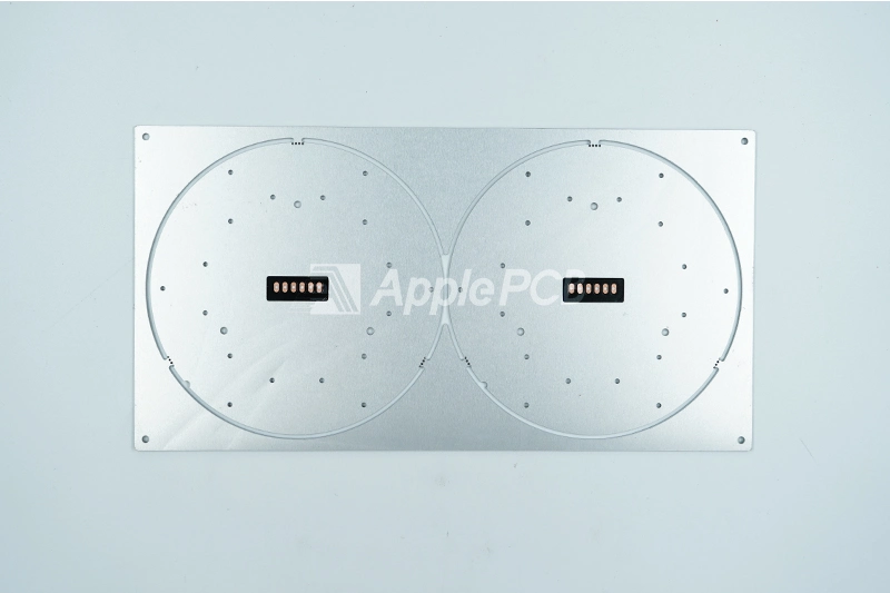
After lamination, the upper copper foil is patterned using photolithography and wet etching processes to form the conductive trace geometries and thermal pad layouts.
- Dry-Film Lamination: A photosensitive dry-film photoresist is laminated onto the cleaned top copper layer under controlled heat and pressure.
- UV Exposure: Gerber-derived photo-artworks are aligned over the dry film. Under high-intensity UV light, exposed sections of the resist cross-link and polymerize into an acid-resistant polymer matrix, while unexposed areas remain soluble.
- Developing: The panel is rinsed with a mild sodium carbonate developer solution to dissolve unpolymerized film, revealing the bare copper zones ready for removal.
- Acid/Alkaline Etching: Chemical etchants dissolve the exposed copper surfaces not shielded by the hardened resist, leaving behind the desired circuit traces and mounting pads.
- Resist Stripping: A strong alkaline bath (typically sodium hydroxide) strips away the remaining resist layer, revealing pristine, bare copper circuits.
Engineering Challenge
Because aluminum PCBs frequently utilize heavy copper weights—3 oz up to 6 oz—to carry large continuous currents, etching poses a significant geometric challenge. As the chemical etchant dissolves copper downward, it also attacks trace sidewalls laterally, a phenomenon known as side etching or undercut.
If etched at a direct 1:1 ratio based on Gerber data, the top of the trace will erode inward, resulting in an undersized conductor cross-section that severely reduces current capacity and alters impedance values.
To overcome this, front-end CAM engineers enforce three strict manufacturing controls:
- CAM Trace Width Pre-Compensation: Traces in Gerber files are expanded in the CAM system based on copper thickness and the material's specific Etch Factor. This ensures that after side etching occurs, the finished trace dimensions hit nominal drawing specs perfectly.
- Micro-Geometric Variance Accounting: Photolithography parameters—including resist thickness, UV light scattering, and film expansion—are calculated to maintain trace geometries well within IPC tolerance limits.
- Etch Factor Optimization: Chemical processing parameters, such as spray nozzle pressure, conveyor line speed, etchant concentration, and bath temperature, are continually monitored to keep undercut ratios minimal.
6.Solder Mask Application & SilkscreenLegend
The solder mask layer protects non-soldering copper traces against environmental oxidation, mechanical scratches, and high-voltage dielectric breakdown, while preventing solder bridging between adjacent SMT pads during automated reflow. The silkscreen legend provides high-contrast component placement reference designators (RefDes), polarity markers, and pin 1 indicators to streamline SMT assembly and optical inspection (AOI).
Engineering Challenge
For heavy copper MCPCBs, applying an even solder mask coat is a major fabrication bottleneck. The substantial height difference between the top of the thick copper traces and the recessed dielectric base creates steep vertical sidewalls.
Using standard single-pass screen printing over heavy copper creates severe defects, such as:
- Trapped air bubbles along copper trace edges.
- Shadowing effect resulting in thin, under-cured ink over sidewalls.
- Inadequate dielectric breakdown voltage at sharp trace shoulders.
Solder Mask Quality Assurance Rules
To ensure a smooth, pinhole-free solder coat with high breakdown resistance, manufacturing operations implement three specialized processing techniques:
- Automotive-Grade LPI Inks: Formulating specialized Liquid Photoimageable (LPI) solder masks engineered for high thermal endurance and strong adhesion to metal core bases (such as high-reflectivity white LPI for LED applications).
- Double-Pass Printing & Curing: Applying two separate LPI coating and soft-bake cycles to ensure uniform encapsulation over thick copper shoulders without sag or pinholes.
- Resin Planarization for Extreme Heavy Copper: For extreme copper weights, a thermally conductive resin is squeegeed between traces, thermally cured, and ceramic-ground flat before solder mask application. This planarization step eliminates micro-voids between tight trace clearances, maximizing electrical insulation ratings.
7.Mechanical Drilling & Plated Hole Metallization
Drilling aluminum core boards requires entirely different feeds, speeds, and tooling compared to standard FR-4 fiberglass. Because the drill must cut through a heterogeneous sandwich of soft copper, dense thermal resin, and tough metallic aluminum, standard drilling recipes will result in rapid tool wear, drill bit breakage, and severe mechanical burrs.
Key Processing Steps
- Precision Mechanical Drilling: Positioning slots, non-plated mounting holes, and thermal/electrical through-holes are drilled into the board. Because aluminum melts at low temperatures and is highly ductile, frictional heat can melt aluminum chips, causing them to weld onto drill flutes and create excessive exit burrs. To prevent this, fabricators use specialized solid tungsten-carbide bits, optimized feeds and speeds, chilled aluminum entry boards, and high-volume vacuum extraction.
- Deburring & Desmear Cleaning: Following drilling, panels pass through heavy-duty mechanical deburring brushes and high-pressure fluid rinses to scrub away exit burrs. Chemical desmear cleaning is then applied to strip away friction-melted resin smear from exposed dielectric hole walls.
- PTH Metallization (For Double-Sided / Grounded MCPCBs): For double-sided aluminum boards or designs requiring direct chassis grounding and thermal vias, hole walls must be made conductive. The non-conductive resin along the hole barrel is first rendered conductive via Electroless Copper Deposition or direct carbon plating. Panels are then electroplated to build up a dense copper barrel wall, forming a low-resistance path for electrical signal ground and direct thermal conduction.
8.Mechanical Profiling & Array Depanelization
After completing circuit patterning, solder mask, silkscreen legend, and surface finishes, the master production panel is milled into individual units or SMT array panels (delivery pallets) tailored for automated pick-and-place assembly.
Outline Fabrication Methods
- CNC Mechanical Routing: High-speed CNC routers fitted with specialized tungsten-carbide end mills cut along complex mechanical contours and cutouts. Routing aluminum requires rigid depth control (Z-axis offset) and low feed rates to prevent metal flashing, thermal tool clogging, or mechanical stress that could cause dielectric layer micro-delamination along the board edge.
- V-Scoring (V-Cut): Precision V-grooves are scored into both the top copper face and bottom aluminum backing for rectangular array designs. Because aluminum alloys are tough, scoring depth tolerance must be tightly maintained:
Too shallow: Depanelization requires excessive mechanical force, risking trace fracture or board cracking.
Too deep: Array panels lose structural integrity, causing severe board sagging or warping under high-temperature SMT reflow ovens.
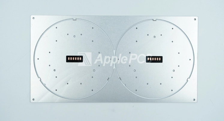
- Breakaway Tabs & Stamp Holes (Mouse Holes): For odd-form or circular board outlines, panels are routed using breakaway tabs integrated with perforated micro-holes (mouse holes). This design maintains structural panel rigidity through SMT stencil printing and component placement while allowing clean, burr-free manual or mechanical depanelization afterward.
9.Inspection, Electrical Testing & Quality Assurance
Prior to final packaging and delivery, every aluminum PCB batch undergoes rigorous electrical, optical, and dimensional inspection to verify structural integrity and electrical performance.
Core Inspection & Test Protocols
- Flying Probe & Bed-of-Nails Testing: 100% electrical continuity and isolation testing is executed across all netlists using flying probe or dedicated bed-of-nails test fixtures. This verifies zero open circuits, micro-shorts, or resistive faults across the patterned copper traces.
- AOI: High-resolution optical cameras paired with automated pattern-matching algorithms scan etched copper and cured solder mask layers. AOI detects subtle microscopic defects such as trace necking, copper slivers, pinholes, mouse bites, and uneven solder mask encapsulation.
- Hole Plating / Cross-Sectioning: For double-sided or plated-through-hole (PTH) aluminum boards, coupon samples are sectioned, mounted in resin, and polished for metallographic inspection. Optical microscopy measures copper plating barrel thickness and checks for micro-voids or interfacial delamination between the thermal dielectric layer and the aluminum substrate.
- Dimensional Inspection & CMM Verification: Optical Coordinate Measuring Machines verify critical mechanical tolerances, including outer profile dimensions, mounting hole locations, notch radii, and remaining V-score web thickness. This ensures flawless mechanical registration during automated SMT pick-and-place and final chassis enclosure mounting.
Final Thoughts
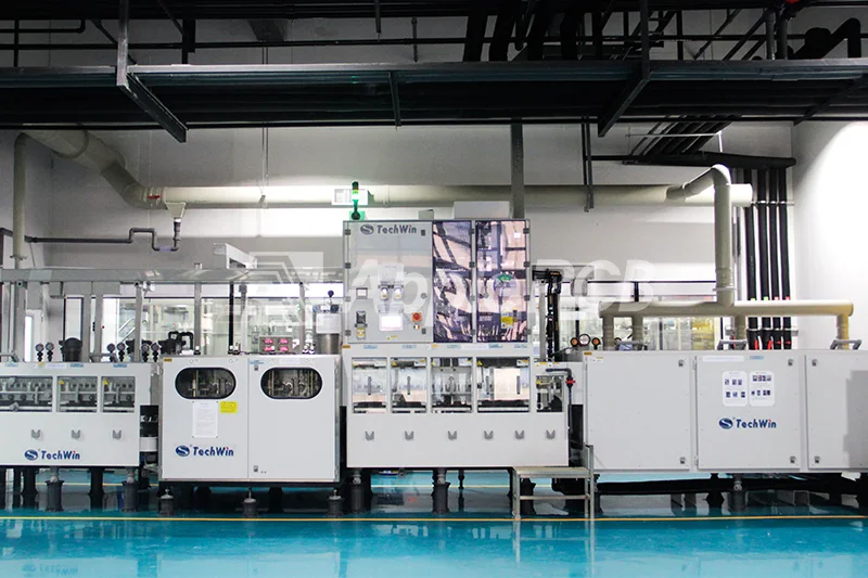
While the overall manufacturing workflow of an Aluminum Core PCB mirrors that of standard FR-4 laminates in many respects, integrating a heavy metal substrate introduces several critical engineering and processing nuances:
- Specialized Surface Pre-treatment & High-Pressure Lamination: Demands micro-texturing and strict process windows to prevent inter-layer delamination under thermal stress.
- Heavy Copper Processing & Compensated Design Rules: Requires precise CAM pre-compensation and controlled etchant chemistry to manage severe side etching on 3 oz+ copper traces.
- High-Temperature Interfacial Bonding: Utilizes specialized thermal dielectrics cured under vacuum lamination to achieve maximum dielectric strength and high thermal conductivity.
- Thermal Mass Sensitivity & Tailored SMT Profiles: High thermal dissipation requires optimized pre-heating profiles during reflow and selective soldering.
- Customized Mechanical Tooling: Demands specialized tungsten-carbide end mills, specific feed/speed recipes, and active dust/chip removal for smooth, burr-free CNC routing and V-scoring.
Partner with ApplePCB
As a specialized manufacturer of metal-core printed circuit boards, ApplePCB operates in full compliance with automotive and industrial-grade quality management systems. Supported by extensive experience in metal-substrate fabrication, our engineering team provides end-to-end support—from front-end DFM reviews and thermal stackup design to fully certified production delivery.
Contact the ApplePCB Engineering Team today to evaluate your design specifications, optimize your stackup, or request a manufacturing quote for your next aluminum core PCB project.