In electronics manufacturing, the precision of the SMT process directly dictates the performance, lifespan, and field reliability of the end product. Achieving a high-yield PCBA run requires uncompromising process control at every single station on the assembly line.
If you have ever wondered how a bare piece of FR-4 transitions into a fully functional, component-dense circuit board, here is a look at the five core stages of the SMT assembly line.
SMT Process Step 1: PCB Fabrication and Incoming Material Inspection
A highly efficient SMT run relies entirely on the quality of the bare boards and the precision of the tooling entering the line. Before a single machine is powered on, both the raw substrates and the production tooling must pass strict engineering audits.
Solder Pad Construction
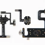
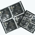
The surface of a bare PCB features an array of flat, non-drilled copper landing areas known as solder pads. These pads form the physical and electrical interfaces that secure the terminals of SMT components, ranging from passive resistors to complex ICs.
To prevent the exposed copper from oxidizing and to guarantee excellent solderability, the factory applies a specific metal coating over these pads. Depending on the application, common surface finishes include:
- HASL (Hot Air Solder Leveling)
- Lead-Free HASL
- Immersion Silver
- ENIG (Electroless Nickel Immersion Gold)
The SMT Stencil: Precision Tooling
Before printing can begin, the factory must produce a custom SMT stencil—often referred to as a laser-cut steel stencil.
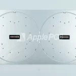
This thin sheet of stainless steel is precisely cut using high-resolution lasers, matching the exact X and Y coordinates of the PCB’s solder pads. The stencil acts as a physical mask, defining the exact boundaries for solder paste deposition and ensuring that paste is applied only where the components will sit.
Incoming Quality Control (IQC)
As the gatekeeper of the SMT assembly line, every material, substrate, and consumable must pass a rigorous quality compliance check before release. This step involves:
- Sampling bare boards to verify flatness (checking for bow and twist).
- Inspecting pad finishes for oxidation or uneven coating.
- Measuring stencil aperture dimensions to ensure volume deposition accuracy.
- Inspecting and logging components to eliminate physical defects before they can jeopardize the assembly run.
SMT Process Step 2: Solder Paste Printing
Solder paste printing is one of the most critical, high-precision processing stages on the SMT line. During this step, an automatic solder paste printer uses the stainless steel stencil and a precision metal squeegee to cleanly deposit paste onto the bare circuit board's pads.
Squeegee Angle and Dynamic Pressure
During the printing stroke, the squeegee blade moves across the stencil under controlled pressure. This action serves a dual purpose: it forces the paste down into the open stencil apertures and shears away excess paste from the top surface of the foil.
To ensure the paste rolls smoothly across the stencil and releases cleanly without slumping, the squeegee's sweep angle must be locked between 45° and 60°.
Solder Paste Characteristics
The solder paste is a putty-like, highly viscous, thixotropic suspension. It consists of microscopic alloy solder spheres suspended in a dense, chemical flux vehicle. The flux serves two distinct, crucial roles:
- Pre-reflow (Temporary Adhesive): It acts as a temporary glue, providing enough wet tack to hold surface mount components (SMDs) securely in place after they are populated on the PCB.
- During Reflow (Chemical Activator): As the temperature rises in the oven, the flux activates chemically to strip away oxidation and impurities from the copper pads and component leads, ensuring a perfect metallic bond.
Volume Control and Joint Formation
The sole purpose of solder paste is to establish a permanent electrical and mechanical bond between the component terminals and the board.
Every pad requires an incredibly precise volume of paste. If the deposition volume is too low, the solder will not form a proper fillet during reflow, leaving you with open circuits or brittle, cold solder joints. Conversely, if the machine deposits too much paste, the excess solder will flow together under heat, creating bridges between adjacent pins (solder bridging) and causing short circuits.
Solder Paste Inspection (SPI)
To catch printing errors instantly, the board is routed directly into an in-line 3D Solder Paste Inspection (SPI) machine.
The SPI system uses laser profiling to measure the exact volume (Volume %), height, and area of the paste deposit on every single pad. If a deposit strays outside of standard tolerances (such as exceeding 130% of the target volume or dropping below 70%), the system immediately triggers an alarm and halts the line. This allows operators to wipe and reprint the board before it ever enters the reflow oven, dramatically improving assembly yield and eliminating difficult post-assembly rework.
SMT Process Step 3: Component Placement
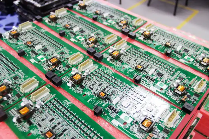
With the solder paste precisely printed, the board moves to the most dynamic, high-speed station on the SMT line: Component Placement. Here, fully automated, computer-controlled pick-and-place machines take over, populating the board by placing SMDs onto their designated pads with absolute precision.
Precision Sourcing and Board Handling
The pick-and-place machine features highly agile placement heads equipped with specialized vacuum nozzles or mechanical grippers. These nozzles use suction to lift components directly from packaging tapes or trays mounted on the machine's feeders.
While the machine preps its nozzles, conveyor belts smoothly transport the paste-printed PCB into the active work zone, locking it securely in place to eliminate any vibration during assembly.
The Balance of Speed and Accuracy
Modern industrial pick-and-place systems achieve an incredible balance of blistering speed and micron-level accuracy. Depending on the machine configuration, high-performance chip shooters can place up to 80,000 components per hour.
To maintain pinpoint accuracy at these speeds, the machine utilizes advanced vision systems. As the placement head moves, upward-looking cameras perform "on-the-fly" optical alignment checks of each component, calculating and correcting any mechanical offsets before the nozzle deposits the component into its exact coordinate on the board.
Tight Tolerances and Cost Control
As modern electronics trend toward high-density, ultra-miniaturized designs (such as 0201 or 01005 passives), the margin for error is virtually zero. Any slight misalignment, rotational skew, or misplaced lead will cause the component to shift or "tombstone" (lift up on one end) when the solder liquefies in the oven.
Catching and fixing these errors post-reflow requires tedious, manual rework that drives up labor costs and risks damaging the board. Keeping placement tolerances exceptionally tight is your first line of defense against production bottlenecks and material scrap.
SMT Process Step 4: Reflow Soldering
Once populated, the conveyor system carries the board into the heart of the SMT line: the reflow soldering oven. By moving through a highly calibrated thermal envelope known as the reflow temperature profile, the assembly passes through four distinct heating zones. This controlled process melts the solder paste and cools it to form solid, reliable metallurgical joints.
Preheat Zone
As the board enters the first chamber of the oven, the preheat zone gradually ramps up the temperature of the PCB substrate, components, and solder paste. To prevent micro-cracking in stress-sensitive ceramic capacitors or warping the laminate due to thermal shock, the heating rate is strictly throttled between 1.0°C/s and 2.0°C/s until the board stabilizes between 140°C and 160°C.
Soak Zone
In this zone, the assembly is held at a steady thermal plateau of 140°C to 160°C for roughly 60 to 90 seconds. The goal here is thermal equalization—ensuring that dense, heavy components (like power inductors) reach the exact same temperature as small, fast-heating passives. Simultaneously, this heat activates the chemical flux within the paste, evaporating volatile solvents and stripping away oxide layers from the copper pads and component leads.
Reflow Zone (Peak Temperature)
This is where the actual liquid metal bonding takes place. The ambient temperature climbs rapidly at a rate of 1.0°C/s to 2.0°C/s, crossing the liquidus point of the solder alloy and peaking between 210°C and 230°C.
Under this extreme heat, the microscopic solder spheres melt completely into a unified liquid pool that wets the component leads and PCB landing pads. During this liquid phase, a remarkable physical phenomenon occurs: the surface tension of the molten solder acts as a self-alignment mechanism, automatically pulling slightly misaligned components back onto the exact center of their pads.
Cooling Zone
The final chamber of the oven functions as a rapid, controlled heat-sink. Its job is to quickly cool and solidify the molten solder before the board exits the machine. Fast, controlled cooling prevents the formation of coarse intermetallic grain structures, resulting in a fine, shiny crystalline joint that delivers superior mechanical shear and tensile strength.
Double-Sided Assembly (Second Pass)
If your layout requires components on both sides, the factory runs the board through a second cycle. The top side is assembled and reflowed first. Then, the board is flipped.
For the second side, the machine prints paste and places components exactly as before. When the board goes through the reflow oven a second time, the surface tension of the molten solder on the underside prevents the already-soldered bottom-side components from falling off. For heavy components on the bottom, the factory may apply small dots of SMT adhesive (glue) prior to placement to lock them mechanically in place during the second pass.
Step 5: Post-Reflow Cleaning and Quality Inspection
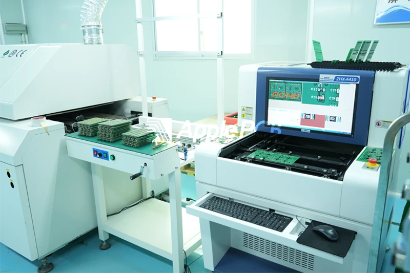
Exiting the reflow oven is not the final step. Before a completed PCBA can be packaged and shipped, it must undergo thorough cleaning to remove chemical flux residues, followed by rigorous quality control. Because modern components are far too small for manual inspection alone to be reliable, factories deploy a suite of specialized optical, mechanical, and X-ray inspection equipment to catch defects before delivery.
Optical Inspection and Microscopy
While automated systems do the heavy lifting, high-power optical microscopes and magnifiers remain critical bench tools. Quality control technicians use them to manually double-check suspicious solder joints flagged by automated machines or to perform random cosmetic sampling across a production batch.
Automated Optical Inspection (AOI)
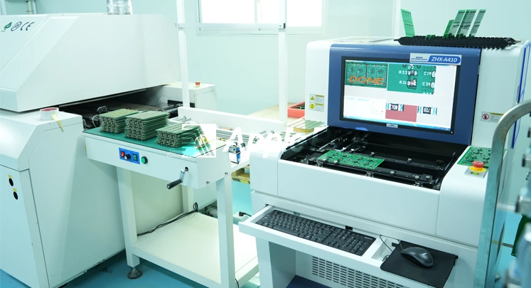
AOI systems are the primary quality workhorses of the SMT line. Positioned directly after the reflow oven, an AOI system uses high-speed, high-resolution cameras and multi-angled LED lighting to capture detailed images of the board surface.
Advanced pixel-comparison and pattern-recognition algorithms compare the captured images against a golden board design file. Within seconds, the system flags cosmetic and structural issues, including:
- Missing components or misaligned parts
- Incorrect component values or package sizes
- Reversed polarity on diodes and ICs
- Tombstoning (components standing vertically on one pad)
- Solder bridging and solder ball defects
Flying Probe Testing
A flying probe tester is a highly flexible electrical test system. It uses a set of high-precision, software-controlled robotic probes that "fly" across the board, making contact with test pads and component leads.
Because the probes are fully programmable, this method requires no physical test fixtures, making it perfect for rapid-turn prototypes and low-volume production. The tester injects electrical signals to measure continuity, open circuits, shorts, and precise passive values like resistance, capacitance, and inductance.
In-Circuit Testing and Functional Testing
For high-volume production runs, flying probe testing is too slow. Instead, factories use custom-built ICT or FCT test fixtures, commonly referred to as a bed of nails.
These fixtures feature a rigid matrix of spring-loaded pogo pins aligned to match every test point on the PCB layout. When the pneumatic press down-clamps the board onto the pins, the system tests the entire circuit simultaneously. This allows the factory to run complete electrical verification and functional firmware tests in a matter of seconds.
Automated X-Ray Inspection (AXI)
With the rise of advanced packages like Ball Grid Arrays (BGAs) and Quad Flat No-leads (QFNs), the solder connections are buried completely beneath the silicon package. Standard optical cameras cannot see them.
To inspect these hidden joints, the factory routes the board through an X-ray inspection chamber. The X-rays penetrate the component packaging, revealing the internal structure of the solder balls beneath. Operators use these high-contrast images to identify hidden shorts, solder bridging, and microscopic voids (air pockets) inside the solder joints, ensuring structural integrity where visual inspection is blind.
Future Trends in PCB SMT
The consumer electronics market's relentless drive toward smaller, thinner, and high-performance hardware is pushing SMT manufacturing tolerances to their absolute limits. Looking ahead, the evolution of surface mount technology is converging on three primary pillars:
Extreme Miniaturization and High-Density Integration: Factory floors are rapidly adapting to handle ultra-miniature passive components (such as 03015 and 008004 form factors) alongside highly complex, multi-layered high-density interconnect (HDI) PCBs.
Smart Factories and Closed-Loop Automation: Artificial intelligence (AI) and machine learning are moving onto the production floor. By establishing closed-loop data connections between SPI, pick-and-place, and AOI machines, modern lines can automatically calibrate placement offsets in real-time and predictively flag defect patterns before they occur.
Green and Sustainable Manufacturing: Stricter global environmental compliance standards are driving the adoption of low-temperature lead-free solders, recyclable fluxes, and energy-efficient reflow ovens, reducing the overall carbon footprint of electronic assembly.
Work with ApplePCB for Your Next Assembly Run
While manufacturing technologies and machinery continue to advance, the core recipe for hardware success remains the same: high yields require uncompromising control over every process step.
If you are searching for a PCBA partner capable of executing complex board layouts under a rigid, zero-defect quality inspection workflow, ApplePCB delivers.
Ready to start your next project? Contact our engineering desk today or upload your Gerber files to our secure system for an immediate, comprehensive quote and a professional DFM (Design for Manufacturability) review.