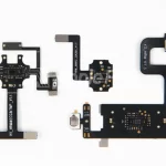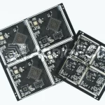
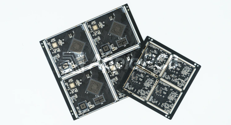
If a finished electronic device is envisioned as a newly constructed building, a bare board PCB serves as its unfinished structural frame.
In simple terms, a bare board contains only the essential conductive elements—copper traces, pads, surface finishes, and plated through-holes—without any ICs, resistors, capacitors, or active/passive components mounted or soldered onto it. Despite its minimalist state, the unpopulated bare board forms the foundational starting point for all downstream PCBA processing, serving two fundamental purposes:
- Mechanical Structural Support: Providing physical mounting locations and structural rigidity to hold components securely.
- Electrical Interconnection: Creating precise copper routing paths and inter-layer vias to distribute power and route high-speed signals between device pins.
As the physical foundation and structural skeleton of any electronic system, bare board fabrication quality directly governs downstream SMT assembly yield, solder joint reliability, and the long-term operational lifespan of the final end product.
Functions of Bare Board PCBs
Before any active or passive components are mounted, the raw unpopulated circuit board serves as the structural and electrical backbone of the assembly. Its primary functions span four key areas:
- Circuit Customization & Functional Scalability
Unpopulated copper traces and pads provide a flexible foundation for hardware designers. Engineers can populate specialized component configurations—including passive resistors and capacitors, discrete transistors, and complex IC packages—to build tailored circuits ranging from simple power regulators to multi-layer processing architectures.
- Streamlined Automated SMT & Through-Hole Assembly
Engineered bare boards integrate precise fiducial markers, tooling holes, and optimized pad geometry designed specifically for high-speed automated assembly lines. This layout standardization enables SMT pick-and-place equipment, stencil printers, and wave soldering machines to position and solder parts with high precision and throughput, driving down per-unit manufacturing costs.
- Educational Demonstration & R&D Prototyping
Without populated components obscuring the substrate, bare boards expose the underlying copper routing paths, power planes, and layer transitions. This transparent structure makes bare boards an excellent tool for academic instruction, board-level signal path analysis, and early-stage R&D layout debugging.
- Front-End Quality Verification via Bare Board E-Testing
Performing quality screening at the bare board stage serves as a critical cost-containment barrier in PCB fabrication. Executing netlist continuity and isolation tests via E-test and automated visual scans via AOI catches substrate defects like trace opens, copper slivers, or short circuits early—ensuring expensive silicon components are never mounted onto defective substrates.
What is Bare Board PCB Testing?
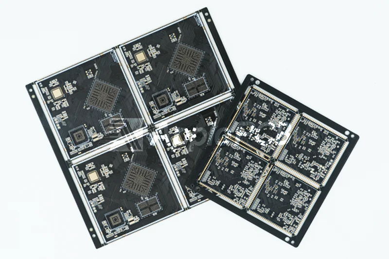
Bare board electrical testing (BBT) relies on two industry-standard probing architectures to verify netlists prior to SMT assembly:
Bed-of-Nails Testing (Dedicated Fixture / ICT): Utilizes a custom test fixture populated with hundreds of spring-loaded pogo pins that press onto test pads across the board simultaneously. Testing an entire panel takes only seconds, making it the standard choice for high-volume manufacturing. However, fabricating custom test heads requires significant non-recurring engineering (NRE) costs and setup lead times, rendering it impractical for quick-turn prototypes.
Flying Probe Testing (FPT): Deploys software-controlled precision robotic arms carrying ultra-fine probe tips that rapidly travel across the board surface to execute point-by-point continuity and isolation checks. FPT requires zero hard tooling—engineers simply load the IPC-D-356 netlist file—offering unmatched flexibility and low startup costs for prototype evaluation, NPI runs, and low-volume production.
What Is the Role of Bare Board Testing?
Bare board testing is a comprehensive inspection executed on raw, unpopulated PCBs to verify electrical continuity, layer isolation, and physical structure before any components are mounted. Catching substrate defects after SMT assembly often leads to complete board scrapping or high-cost manual rework.
Executing BBT during early fabrication yields three primary operational advantages:
- Screening Electrical Faults
The primary objective of BBT is detecting latent electrical defects—such as trace opens, copper shorts, micro-cracks, and poor pad integrity—across the bare copper network. Screening unpopulated boards prevents defective substrates from entering downstream SMT assembly.
- Verifying Netlist Integrity & Layer Interconnects
BBT validates that all signal paths, power planes, and blind/buried vias align precisely with the original Gerber or IPC-D-356 netlist design files. In complex multi-layer stackups, electrical testing verifies seamless z-axis interconnectivity across internal layers, catching missing connections or etch defects early.
- Cost Mitigation & Scrap Reduction
Detecting bare board flaws at the bare substrate stage prevents high-value ICs, microcontrollers, and passive components from being soldered onto defective boards. Early screening avoids mass scrap, eliminates manual rework costs, and stabilizes production lead times.
Comparison Between Zero PCB and Bare PCB
Zero PCB (also known as perfboard or DOT PCB) and bare PCB show significant differences across multiple dimensions:
- Definition and Structural Function: Zero PCB is a general-purpose board without preset functions, circuit connections, or layouts; bare PCB is a standard board that has not yet had any electronic components installed.
- Trace and Pad Design: Zero PCB has no preset copper traces and requires users to manually solder and wire later; bare PCB is strictly based on design files, printed with predefined and precise copper traces and pads.
- Protective Layer and Silk Screen: Zero PCB boards do not include solder mask layers or silkscreen legend layers; bare PCB completely possesses both solder mask and silkscreen layers.
- Appearance and Layout: Zero PCB presents a perforated structure with a grid array; bare PCB has specific dimensions and a pre-designed circuit layout.
- Customization and Design Flexibility: Zero PCB provides user-driven design flexibility and can be used off the shelf; bare PCB must be customized during the factory manufacturing process to precisely match specific circuit design requirements.
- Manufacturing and Processing Technology: The manufacturing process of Zero PCB is relatively simple; bare PCB requires submitting detailed PCB design drawings and is processed through complex industrial-grade manufacturing steps.
- Core Application Scenarios: Zero PCB is mainly used for educational experiments, personal DIY, and early-stage circuit prototype testing; bare PCB serves as a test substrate prior to large-scale mass production, as well as the core baseboard for final component assembly.
Selecting the Right Bare Board PCB Manufacturer
As a dedicated partner in high-reliability electronics manufacturing, ApplePCB delivers end-to-end bare board fabrication services—spanning early-stage PCB layout design and material sourcing to rapid turnaround prototyping, high-volume SMT assembly, and comprehensive electrical testing. Integrated with intelligent MES and ERP shop-floor tracking systems, ApplePCB leverages automated high-precision inspection tools to enforce strict process control at every stage of production.
ApplePCB supplies bare boards across mission-critical sectors including automotive electronics, medical systems, smart home devices, and high-power telecommunications infrastructure. Operating in full compliance with ISO 9001, IATF 16949, and ISO 13485 quality management frameworks, ApplePCB's engineering and quality control teams provide round-the-clock technical support to optimize client designs.
Backed by over 15 years of fabrication expertise and manufacturing innovation, ApplePCB guarantees industry-leading yield, substrate reliability, and strict compliance. Contact the ApplePCB engineering team today to request a complete Gerber file DFM review and an accurate manufacturing quote for your next hardware design.