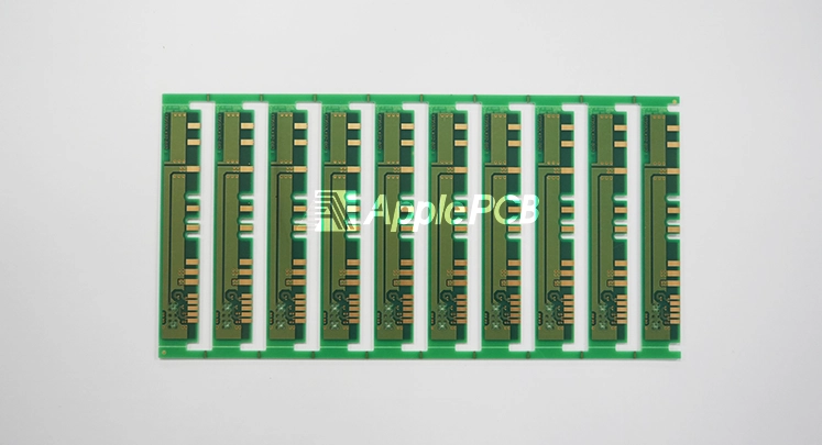
A Bluetooth PCB is a specialized printed circuit board engineered specifically for short-range wireless communication. By integrating RF transceivers, microcontrollers, matching networks, and onboard or chip antennas onto a single board, a Bluetooth PCB enables seamless wireless data exchange between devices without physical cable interconnections. From smartphones and wireless earbuds to IoT smart home hardware, these compact RF circuit assemblies serve as the core hardware foundation for modern short-range wireless connectivity.
How a Bluetooth PCB Works?
A Bluetooth PCB integrates a Bluetooth System-on-Chip, RF matching components, crystal oscillators, power management circuits, and printed or chip antennas into a compact footprint. Component placement and trace routing are strictly engineered to maximize RF signal strength, minimize electromagnetic interference, and control power dissipation. Optimized board layouts lower fabrication costs, improve assembly yield rates, and simplify downstream testing and maintenance.
Functionally, a Bluetooth PCB controls bi-directional RF signal transmission and reception, ensuring reliable data exchange between paired hardware nodes. The board's RF frontend filters out out-of-band noise, modulates baseband digital signals into the 2.4 GHz ISM frequency band, and handles secure cryptographic handshakes to prevent unauthorized data interception.
Types of Bluetooth PCB Modules
Bluetooth modules can be broadly categorized into three types based on function: data transmission modules, audio modules, and audio + data modules.
Data Transmission Bluetooth PCB Modules
This class of module focuses on the wireless transmission of non-audio data between devices, making it ideal for application scenarios where the primary requirement is exchanging information rather than audio streams.
A typical data transmission module generally consists of several key components: a Bluetooth transceiver responsible for connecting to peripheral devices, an antenna for transmitting and receiving signals, a microcontroller for data processing, along with interface ports and power management. Taking the common serial transparent transmission module as an example, it typically operates as a slave device. Upon pairing with a host device such as a smartphone or computer, it enables transparent pass-through—data received via the serial port is transmitted wirelessly, while data received over the air is delivered directly through the serial port without alteration. This eliminates the need for developers to write dedicated Bluetooth protocol code within the primary microcontroller firmware.
These modules are suitable for scenarios requiring device-to-device information exchange, such as file transfers, inter-microcontroller communication, and general-purpose wireless data links.
Audio Bluetooth PCB Modules
Audio modules are engineered specifically for the wireless transmission and reception of high-quality audio signals. These modules typically integrate audio codecs and advanced signal processing capabilities to ensure stable connectivity and clear audio output.
Their standard architecture includes power amplifiers, codecs, audio input/output interfaces, microcontrollers, and supporting components such as power management circuits. Select audio modules also incorporate integrated MP3 decoding functions, supporting wireless audio streaming while featuring onboard power amplifiers to directly drive speakers, alongside multiple control interfaces and built-in equalizers.
Audio modules are primarily deployed in wireless audio systems, speakers, headphones, and other devices that demand continuous, high-fidelity audio streaming.
Audio + Data Bluetooth PCB Modules
This class of module combines both data transmission and audio processing capabilities, making it ideal for applications requiring simultaneous audio streaming and general-purpose data communication.
Audio + data modules typically support multiple Bluetooth profiles to fulfill diverse functional requirements concurrently. For instance, smart audio devices can receive control commands or exchange telemetry data while actively streaming audio. Advanced modules integrate audio streaming, audio processors, hardware codecs, and serial control interfaces into a single architecture, delivering a comprehensive solution for applications demanding integrated wireless audio playback and data links.
These modules are widely deployed in smart home speaker systems and connected audio appliances, where they stream high-fidelity audio from source devices while seamlessly exchanging data with other smart nodes across the network.
How to Choose the Right Bluetooth PCB Module?
When selecting a Bluetooth module for a project, the following key factors should be evaluated step-by-step:
- Communication Range: The required coverage range directly determines the module's power class and RF output power. Extended range typically entails higher power consumption and hardware costs. It is best to define power requirements based on real-world operational needs rather than over-specifying for maximum distance.
- Power Consumption: Focus on evaluating the module's current draw across active, idle, and deep sleep states. Pay close attention to parameters like wake-up latency, broadcast interval, and advertising parameters, as these configurations dictate the trade-off between responsiveness and energy efficiency. Always consult the technical datasheet to verify typical and maximum current specifications across transmit, receive, standby, and sleep modes.
- Firmware and Software Support: Verify whether the module supports familiar development environments, such as Arduino, Python, or vendor-specific IDEs. Additionally, assess the vendor's documentation, software development kits, and community ecosystem support. Mainstream silicon vendors generally offer more robust software stacks and reference code in this regard.
- Regulatory Certification: Pre-certification directly impacts time-to-market and compliance budgets. Choosing a module pre-certified for FCC, CE, IC, and Telec significantly streamlines the end-product compliance testing process, eliminating redundant RF testing fees and qualification risks.
- Data Rate and Throughput: Evaluate the module's maximum theoretical throughput versus realistic application payloads, as field performance will be lower than raw interface speeds. For applications that only transmit small, periodic telemetry packets, Bluetooth Low Energy offers sufficient data rates with vastly reduced power consumption.
- Interface Compatibility and Peripherals: Confirm that the module's operating voltage levels match the rest of the system architecture. Depending on the host microcontroller scheme, select a module providing the required digital interfaces, such as UART, SPI, or I2C.
6 Points to Pay Attention to When Designing a Bluetooth PCB
When designing a Bluetooth PCB, evaluating the following engineering considerations during early layout will eliminate significant troubleshooting and debugging friction downstream:
Isolate Copper Signals and High-Energy Components
Within the antenna keepout zone of a Bluetooth chipset or module, all copper signal traces, ground planes, and high-energy components must be completely excluded—particularly switching power supply paths like buck or boost converters.
Furthermore, no ground planes or copper pours should exist on any layer directly beneath or around the antenna keepout area. Most Bluetooth silicon vendors specify precise layout clearance guidelines, which must be strictly implemented. When designing custom antenna keepout layouts, implement ground plane cutouts while maintaining appropriate ground reference regions to preserve input bandwidth and reserve adequate physical real estate for RF tuning networks (both PCB trace antennas and ceramic chip antennas require an adjacent ground reference).
Placing stitching vias along ground plane edges prevents peripheral board edge radiation from coupling into sensitive 2.4 GHz RF paths. Where possible, optimize the board outline to position the Bluetooth SoC and antenna immediately adjacent to the panel edge, maximizing physical separation from noisy digital logic and high-speed traces. When mixing analog circuits (such as audio lines), enforce strict split analog and digital ground topology. In addition, fitting metallic RF shielding cans over core circuitry (excluding the antenna) effectively mitigates cross-coupling and radiated noise.
Pay Attention to Power Supply Design
Power supply rails feeding the Bluetooth module or SoC must remain ripple-free and low-noise. Position 1.0 µF bypass capacitors alongside 0.1 µF and 10 nF decoupling capacitors as close to VDD supply pins as possible. Additionally, inserting a high-frequency ferrite bead in series with the main power rail entering the Bluetooth RF section suppresses high-frequency power plane noise.
Prioritize Using Pre-Certified Modules
For resource-constrained engineering projects prioritizing rapid time-to-market, deploying fully pre-certified Bluetooth modules is highly advantageous. Although integrated modules carry higher bill-of-materials (BOM) unit costs, they bypass complex antenna matching, RF layout optimization, and electromagnetic compatibility (EMC) sensitivity risks.
Numerous cost-effective certified modules are readily available, featuring integrated low-power ARM Cortex microcontrollers—such as Microchip's RN4020 / RN4870 or Silicon Labs' BT121 / BGM113. Integrated microcontrollers provide flexible processing power to drive peripherals via GPIO, SPI, I2C, and PWM interfaces while executing onboard Bluetooth protocol stacks autonomously.
Confirm the Bluetooth Device Matches the Application Scenario
Select Bluetooth hardware tailored precisely to your application profile, ensuring the antenna geometry and RF tuning are optimized accordingly.
For simple beacon deployments—such as periodic or short-burst location and telemetry broadcasting—adopting a low-cost Bluetooth Low Energy (BLE) architecture with minimal peripheral overhead conserves board real estate and minimizes BOM costs.
For applications demanding high data throughput, real-time audio streaming, or heavy packet exchange, specify modules featuring elevated RF output power, higher receiver sensitivity, and faster data rates. Note that moderately reducing operational throughput often lowers overall packet error rates (PER).
If an integrated System-on-Chip (SoC) is preferred, select solutions embedding a high-performance application processor or coprocessor. These SoCs provide robust hardware interfaces, including UART, SPI, I2C, PWM, ADC, DAC, and GPIOs. If your system relies on Received Signal Strength Indicator (RSSI) metrics for location tracking or distance estimation, verify that the module delivers sufficient dB resolution and measurement accuracy.
Consider Barriers in Real-World Environments
In real-world operating environments, multiple path-loss factors can attenuate Bluetooth RF signals or detune matching networks. These include water bodies (including the human body), metallic enclosures, mobile devices, computers, co-channel 2.4 GHz interference sources (such as microwave ovens and Wi-Fi networks), power supplies, wireless video transmitters, fluorescent office lighting, and cordless phones.
Signal attenuation can occur even at short line-of-sight distances (1–2 meters). When operating in high-interference environments, choose higher-power transceiver modules and configure them for lower data rates to maintain link margin and reduce packet retransmissions. If housing the PCB inside a custom enclosure, eliminate metallic plating or conductive coatings in close proximity to the BLE module. The correlation between Bluetooth signal strength and distance is highly non-linear and environment-dependent, though it generally follows log-distance path loss models.
Utilize Suitable Tools and Analysis Methods
When designing custom onboard PCB antennas or matching circuits, ensure access to vector network analyzers to characterize return loss and tune impedance matching networks. If specialized RF equipment is unavailable, submit the layout to a certified third-party RF testing laboratory for antenna tuning and EMC compliance validation.
Bluetooth PCB Pricing
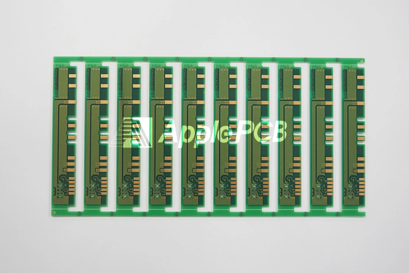
There is no fixed single price point for a Bluetooth PCB. Final fabrication costs depend on several engineering and production variables, including layer count, stackup complexity, RF impedance control tolerances, regulatory certification requirements, and volume scale.
Taking standard rigid FR-4 substrates as a baseline:
- 1 to 2-Layer Bluetooth PCBs: Initial prototype sampling typically ranges from 2 to 5 USD per panel.
- 4-Layer Bluetooth PCBs: Prototype sampling ranges from 10 to 30 USD, dropping to 5–15 USD per unit for low-volume production runs.
- High-Volume Production: For large-scale manufacturing runs, unit fabrication costs for standard Bluetooth PCB designs can drop as low as 1 to 5 USD per unit.
Final Thought
If you are developing a new Bluetooth PCB project—whether at the initial prototype stage or preparing for full-scale production—contact ApplePCB for a custom quotation. Our engineering team provides transparent, competitive pricing based on your Gerber files, stackup specifications, order volume, and fabrication requirements.