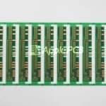

Dual in-line package, sometimes also called DIL packaging. Simply put, it is that kind of electronic component with a rectangular shell and a row of parallel downward pins on each side. When installing, the pins pass through the holes of the printed circuit board and are then soldered on the back side of the board. Generally, the number of pins of this type of device will not exceed 100.
Many people will ask, are DIP and SMT the same? Strictly speaking, they are not.
SMT is surface mount technology, where components are directly mounted on the surface of the circuit board, relying on solder paste printing and reflow soldering. DIP is the through-hole process, usually fixed using wave soldering or manual soldering (also known as post-soldering).
Although both processes belong to printed circuit board assembly processing, the actual situation is that not all printed circuit board assembly factories can do DIP post-soldering well. The difference in processing quality is actually quite large.
From our perspective as a manufacturer, we give you the most practical advice: when choosing a printed circuit board assembly factory to cooperate with, it is best to visit the factory in person. Look at the technical level of the on-site personnel, look at the processing equipment, and experience the overall environment of the workshop. These things often determine whether your boards can ultimately be delivered with guaranteed quality and quantity.
1.Preparation Before Through-Hole Insertion
Material Inspection
Begin by cross-referencing the bill of materials to ensure all component part numbers and technical specifications strictly conform to the schematic design. Verify that 100% brand-new, factory-original components are utilized to prevent common soldering defects. Next, inspect component leads for surface oxidation or mechanical deformation, and confirm that circuit board pads are clean and free of contamination or damage.
Tools and Environment
Soldering iron temperatures must be calibrated between 230°C and 300°C, with premium rosin flux and solder wire prepared. Assembly floors require strict electrostatic discharge protection; operators must wear grounded wrist straps while maintaining adequate workspace ventilation.
Component Preprocessing
Form component leads to precisely match the hole pitch of the printed circuit board, keeping mechanical tolerances within ±0.2 mm. When trimming leads prior to assembly, ensure that the post-soldering lead protrusion length extends 1.5 to 2 mm past the pad surface to guarantee secure mechanical anchoring and joint integrity.
2.Through-Hole Component Insertion
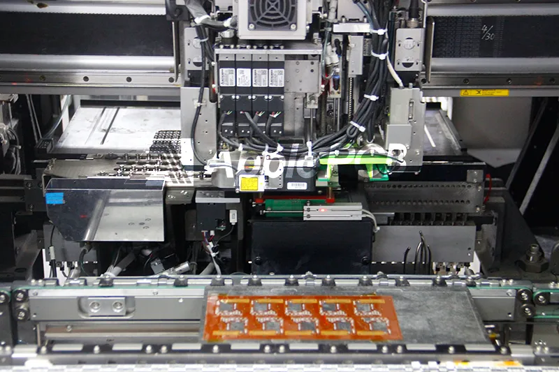
Manual Insertion
Align component leads precisely with circuit board silkscreen designators before insertion. Components must sit flush against the substrate surface without skewing. As a standard assembly practice, populate larger structural components first and reserve delicate or sensitive parts for final placement.
Automated Machine Insertion
For high-volume production runs, automated axial and radial insertion equipment is programmed to populate standard components such as resistors and capacitors with exceptional speed and throughput.
Temporary Securing
Following insertion, utilize dedicated assembly fixtures or high-temperature polyimide tape to secure components firmly in place. This mechanical retention is especially critical for irregularly shaped or tall components, preventing positional shift or lifting during wave soldering operations.
3.Soldering Operations
Wave Soldering
Executed across three distinct thermal zones:
- Preheat Zone: Temperatures are regulated between 100°C and 150°C to activate chemical fluxes, minimize thermal shock to components, and promote smooth solder wetting and intermetallic bonding.
- Peak Soldering Zone: The molten solder pot temperature is maintained between 230°C and 260°C, with wave heights adjusted to submerge approximately two-thirds of the component lead length.
- Cooling Zone: Forced air cooling solidifies newly formed solder joints rapidly before board exit.
Manual Soldering
Technicians follow a rigorous five-step soldering protocol: heating the pad and lead simultaneously, applying solder wire, allowing the alloy to wet the joint, withdrawing the wire, and removing the iron tip. Acceptable joints must exhibit a bright, concave conical shape without burrs, bridging, or cold solder defects.
4.Post-Processing and Quality Assurance
Lead Trimming
Excess component leads are sheared using specialized pneumatic cutters, preserving a minimum lead protrusion of 1 millimeter above the apex of the solder fillet.
Residue Cleaning
Assemblies undergo ultrasonic aqueous or solvent cleaning cycles to eliminate corrosive flux residues and ionic contamination completely.
Rigorous Inspection Protocols
Multi-tier quality gates verify final board integrity:
- Visual Inspection and AOI: Evaluates joint completeness, component placement accuracy, and short-circuit absence.
- X-Ray Inspection: Inspects internal barrel fill and hidden joints beneath dense packaging or shielding.
- Functional Testing: Powers up assembled boards to validate comprehensive electrical performance under operational loads.
5.Critical Process Control Points
- Thermal Management: The temperature delta between the wave soldering preheat zone and the peak soldering zone must not exceed 100°C to prevent printed circuit board delamination or substrate warping.
- Immersion Duration: Lead-to-solder wave contact time should be maintained between 3 and 5 seconds. Insufficient dwell time leads to cold solder joints, while excessive duration risks thermal damage to sensitive components.
- Environmental Protection: For high frequency or high-voltage assemblies, apply a protective conformal coating following through-hole soldering to enhance moisture resistance, insulation, and long-term reliability.
- Process Flow Sequencing: Crucially, through-hole post-soldering operations must integrate seamlessly with surface mount lines. Standard manufacturing practice dictates completing surface mount reflow processes prior to through-hole insertion, preventing thermal reflow exposure from damaging previously placed surface mount devices.
Through-Hole Soldering Defects and Corrective Actions
Even with advanced manufacturing equipment, through-hole post-soldering lines occasionally encounter surface defects. Recognizing, repairing, and preventing these flaws is essential for maintaining strict quality control. Below are five of the most common through-hole soldering defect phenomena.
Solder Bridging and Short Circuits
Visual Defect and Identification: Adjacent solder joints that should remain electrically isolated are connected by a bridge of solder. This defect is unacceptable and requires immediate manual rework or touch-up.
Operational Impact: Directly compromises electrical circuit performance and, in severe cases, causes catastrophic component short-circuit failures.
Root Causes:
Multiple factors contribute to bridging, including insufficient board preheating temperatures, excessive conveyor belt speeds resulting in inadequate wetting time, or incomplete flux activation. Additional causes include excessive board immersion depth into the solder wave, heavy oxide accumulation on the solder pot surface, overly tight component spacing, or improper board transit orientation relative to the flow direction of the solder wave.
Corrective Actions:
Address these issues by raising preheating temperatures, reducing conveyor speeds, and validating board thermal profiles using a specialized profiler. Replenish or replace exhausted flux. Adjust the solder wave height to submerge approximately half of the board thickness and regularly skim oxides from the solder pot. For layout-induced bridging, modify the circuit board design to increase component spacing or adjust the entry angle into the wave to prevent parallel rows of pins from exiting the solder simultaneously.
Solder Skips and Missing Solder Joints
Visual Defect and Identification: Component leads lack proper solder wetting around their circumference, failing to form a complete solder fillet. This defect is unacceptable and mandates immediate touch-up or rework.
Operational Impact: Results in open circuits and complete functional failure. Intermittent solder skips are particularly dangerous because they may pass automated electrical testing only to fail later in the field, creating severe reliability risks for end users.
Root Causes:
Causes include uneven flux foaming or insufficient activation; dense component placement triggering a solder wave shadow effect where trailing components are blocked by leading ones; thermal board warpage; an inadequately low or turbulent solder wave; contaminated component leads; board oxidation or solder mask bleeding onto pads; or excessive conveyor transit speeds.
Corrective Actions:
Optimize flux foam tank air pressure and schedule regular cleaning; recalibrate preheating temperatures and conveyor speed profiles; add thermal or air relief vias in high density layout zones; reposition assembly fixtures; raise solder wave height and clear dross accumulation frequently; replace contaminated components or extend dwell time; clean ink contamination off pads or reject defective boards; and fine-tune conveyor speeds.
Excessive Lead Protrusion Length
Visual Defect and Identification: Component leads extend beyond the allowable protrusion limits past the apex of the solder fillet.
Protrusion limits are governed by lead diameter: for wire diameters ≤0.8mm, protrusion must not exceed 2.5mm; for wire diameters > 0.8mm, protrusion must not exceed 3.5mm.Operational Impact: Excessive lead length encourages solder joint fatigue cracking, starves the fillet of proper solder volume, and risks violating statutory electrical safety clearance specifications.
Root Causes:
Leads protrude excessively due to tilted component insertion during manual placement or incorrect lead-trimming specifications during prep processes.
Corrective Actions:
Enforce vertical alignment during component placement using alignment fixtures to prevent tilting; recalibrate pre-forming lead trimming machines to meet precise length tolerances; and enforce strict upper and lower inspection thresholds during post-soldering quality checks.
Cold Solder Joints
Visual Defect and Identification: Solder joint surfaces appear dull, grainy, or wrinkled rather than smooth and shiny. In severe cases, fractures form around the component lead. This defect is unacceptable and requires immediate touch-up or rework.
Operational Impact: Cold solder joints exhibit poor mechanical strength and short operational lifespans. They are prone to micro-cracking under thermal cycling or vibration, eventually causing intermittent or total circuit failure.
Root Causes:
Typically caused by mechanical vibration while the solder alloy is solidifying (such as excessive conveyor belt vibration); heavy surface oxidation on component leads or circuit board pads; or insufficient wetting dwell time.
Corrective Actions:
Identify and eliminate mechanical vibration sources along the conveyor and soldering line; inspect component leads and pads for oxidation, pre-cleaning or flux-dipping contaminated parts prior to wave soldering when necessary; and decrease conveyor transit speed to extend wetting dwell times.
Pinholes and Blowholes
Visual Defect and Identification: Tiny pinhole-sized cavities appear on the surface of the solder joint. This defect is unacceptable and mandates immediate touch-up or rework.
Operational Impact: Degrades visual appearance and reduces the structural mechanical strength of the solder joint.
Root Causes:
Trapped moisture within the printed circuit board substrate; component leads contaminated with release agents or silicone oils; or air trapped inside plated through-holes that is blocked by component bodies and unable to vent during wave soldering.
Corrective Actions:
Bake circuit boards in an oven at 80°C to 100°C for 2 to 3 hours prior to assembly to eliminate absorbed moisture; strictly enforce handling protocols to prevent bare-hand contact with board surfaces; evaluate component lead forming and placement to prevent blocking barrel venting, and verify that plated through-hole diameters are properly matched to component lead thicknesses.
Final Thoughts
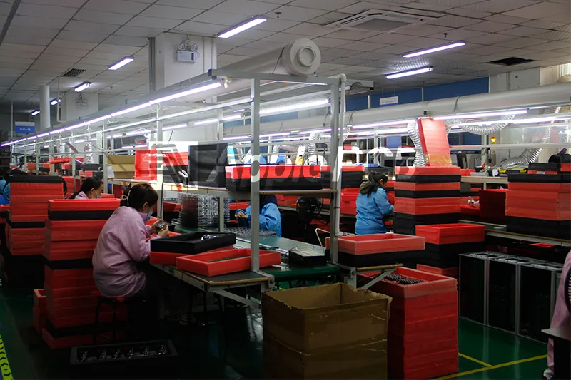
Ultimately, while through-hole post-soldering is a mature, traditional manufacturing process, it demands meticulous attention to detail. Solder bridging, skipped joints, excessive lead length, cold solder joints, and pinholes—these seemingly minor joint flaws directly dictate the maximum quality ceiling of an entire production run. In practical manufacturing, most of these issues can be prevented through rigorous process discipline. Success relies entirely on whether your assembly partner enforces mature manufacturing standards and possesses the engineering expertise to diagnose and resolve floor anomalies quickly and accurately.