With the emergence of advanced packaging technologies like chip-scale packages (CSP) and ball grid arrays (BGA), the demand for IC substrates has surged. For electronic engineers and designers, it’s no longer enough to simply understand the role of IC packaging materials. A deeper understanding of the manufacturing process of IC substrates, the critical role they play in electronic devices, and their specific applications is good to advancing your design expertise.
This article will explore the fundamentals of IC substrates, their material properties, and the manufacturing processes involved, providing you with the knowledge needed to fully grasp the technical background and future potential of this crucial component.
What is an IC Substrate?
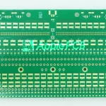
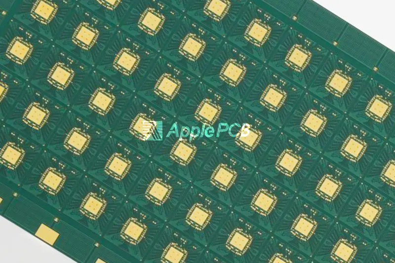
An IC substrate (packaging substrate) is a specialized carrier designed for high-density packaging of integrated circuits. It connects bare chips to the substrate using methods such as solder balls, bumps, or micro blind holes, and the substrate is then linked to the system motherboard or PCB.
In essence, the IC substrate serves three primary functions: supporting the chip, providing electrical connections, and facilitating system installation. The advancement of IC substrate technology, particularly driven by cutting-edge packaging solutions like BGA (Ball Grid Array) and CSP (Chip Scale Package), has led to its rapid adoption in the industry.
IC Substrate vs PCB
IC substrates, which offer higher-density packaging, are designed with greater precision and functionality compared to traditional PCBs. IC substrates typically have 2 to 10 layers, HDI boards range from 4 to 16 layers, and standard PCBs can exceed 100 layers. IC substrates are much thinner, usually no more than 1.5mm thick and can be as thin as 0.1mm, while standard PCBs can be thicker than 7mm. The key parameters are line width and spacing, with IC substrates typically having line width/spacing under 30μm/30μm. In contrast, for regular PCBs, a line width/spacing of 50μm/50μm is already considered to be high-end.
Types of IC Substrates
Classification by Material
IC substrates are generally made from three types of base materials: BT substrates, ABF substrates, and MIS substrates.
1.BT Substrate
BT (Bismaleimide Triazine) is a resin material known for its resistance to thermal expansion, dimensional stability, rigidity, and relatively coarse lines. With excellent thermal and electrical properties, BT substrates are used in applications such as mobile MEMS, storage devices, RF chips, and LED chips.
2.ABF Substrate
ABF is a high-performance film material that offers high hardness and excellent insulation. It is particularly suitable for fine lines, high-layer count, and multi-pin IC packaging. ABF substrates are commonly used in packaging high-performance components like CPUs, GPUs, and chipsets.
3.MIS Substrate
MIS substrates feature one or more layers of pre-packaged structures, with interconnections made via copper electroplating. These substrates offer extremely fine lines, superior electrical performance, and a compact size, making them ideal for analog ICs, power ICs, and applications in the digital currency sector.
Classification by Packaging Type
1.WB/FC
●WB (Wire Bonding):Wire Bonding is a traditional packaging method where fine metal wires are used to connect the bare chip to the substrate. The process involves using heat, pressure, and ultrasonic energy to attach the wires to both the chip pads and substrate pads, creating electrical connections. This method is commonly used in packaging RF modules, memory chips, and MEMS (Micro-Electromechanical Systems) devices, especially for wireless RF power amplifiers, transceivers, and similar components.
●FC (Flip Chip):Flip Chip technology is typically used for high-performance chips like CPUs and GPUs. In this method, the chip is flipped upside down, and solder balls are used to make the electrical connections between the chip and the substrate. Compared to wire bonding, flip chip packaging offers higher signal density and improved chip performance. Additionally, the use of solder balls allows for more precise alignment and results in higher production yields.
2.BGA/CSP
●BGA (Ball Grid Array):In Ball Grid Array (BGA) packaging, solder balls are placed at the bottom of the chip, replacing traditional metal pins. This increases the spacing between I/O terminals and allows for more I/O connections. The main benefits of BGA include high packaging density, excellent yield, and superior electrical performance. It is commonly used for packaging high-performance processors in PCs and servers.
●CSP (Chip Scale Package):Chip Scale Package (CSP) is a packaging form that closely matches the size of the bare chip, with the package area being no more than 1.14 times the size of the chip. CSP is about one-third the size of a traditional BGA, reducing the overall package size significantly.
IC Substrate Manufacturing Methods
The manufacturing methods for IC substrates differ significantly from traditional PCB processes. Traditional PCBs primarily use a subtractive method, where copper is plated onto a laminate, covered with a protective layer, and then etched to remove excess copper. However, during etching, lateral copper corrosion occurs, which limits the precision of the lines, usually preventing them from achieving widths and spacings smaller than 2 mils.
To meet the more precise requirements for IC substrates, advanced methods such as the additive process and the modified semi-additive process are used.
Additive Process (AP)
Unlike the subtractive process, the additive process doesn’t rely on etching. Instead, the circuit is exposed to a photosensitive catalyst, and copper is chemically deposited to form the circuitry. This process allows for much higher precision, with line widths and spacings as small as 1 mil or less.
Modified Semi-Additive Process (MSAP)
The MSAP process improves upon traditional electroplating by using thin copper layers that are built up through plating and then etched to remove excess material. With thin copper layers, etching times are reduced, minimizing lateral corrosion and resulting in finer lines. The MSAP process is more cost-effective than the additive process and offers higher yields for fine lines compared to the subtractive process, making it highly favored.
IC Substrate Manufacturing Challenges
1.Line Width/Spacing
Standard HDI PCB line widths are typically 75μm, but IC substrates need to handle far smaller widths of 10-25μm to accommodate the dense I/O pin configurations of modern chips. These lines are so fine they are even thinner than a human hair.
2.Microholes
Traditional PCBs use laser drilling with hole sizes larger than 100μm, while IC substrates require microholes smaller than 50μm. These holes must be filled with copper to ensure reliable electrical connections and to maintain a smooth surface for the next layer.
3.Materials
Standard FR-4 materials are not suitable for IC substrates due to their high thermal expansion and electrical loss. Instead, advanced materials like BT (Bismaleimide Triazine) resin and ABF (Ajinomoto Build-up Film) are needed for IC substrate production.
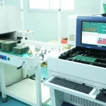
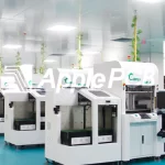
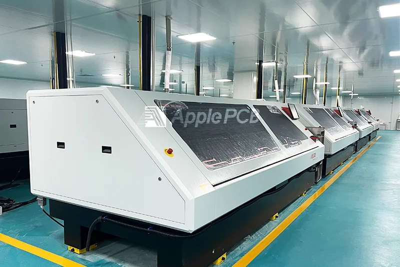
How ApplePCB Overcomes IC Substrate Manufacturing Challenges
With 15 years of experience, ApplePCB constantly enhances its manufacturing technologies and equipment to meet the precision demands of IC substrate production. We use advanced mSAP and AP processes, high-precision electroplating, laser drilling, and ultra-thin laminating equipment to ensure that every IC substrate meets the highest precision standards.