In PCB design, trace width and spacing—these seemingly simple design elements—are often overlooked. Yet they profoundly impact the product. An improper trace design can not only lead to unstable board performance but also cause quality issues during production, potentially affecting the end product's lifespan. We will clarify why trace width matters through several key points.
●Electrical Safety
If high-voltage traces are too close together, breakdown can easily occur, potentially triggering arcing. Maintaining proper widths and spacing reduces risks and ensures safety.
●Signal Quality
Insufficient spacing causes crosstalk, where signals interfere with each other. This results in unstable high-speed circuits and distorted analog signals. Proper routing design ensures cleaner, more intact signals.
●EMI/EMC Compliance
Appropriate routing spacing effectively reduces electromagnetic interference, making products easier to pass EMC testing and avoiding rework and extra costs.
●Impedance Matching
High-speed transmission demands strict impedance control. Only when trace width and spacing are properly managed can signals transmit stably without reflection or loss.
●Thermal Management & Lifespan
Particularly for power traces, insufficient width or spacing causes heat buildup, accelerating board degradation. Designing with margin ensures circuit durability.
●Manufacturing Reliability
PCB fabrication is a precision process with inherent manufacturing tolerances. Excessively narrow traces or insufficient spacing can cause defects like shorts or breaks. Adhering to design rules ensures stable mass production.
●Design for Testability (DFT)
Adequate spacing facilitates probe testing and debugging later in the process, reducing test time.
Key Factors That Determine PCB Trace Width
1.Current Capacity
A trace must be wide enough to safely carry the required current. The higher the current, the more heat the trace produces. If the trace is too thin, heat builds up, raising the temperature and potentially burning or delaminating the copper. In short, a wider trace means better current capacity and improved reliability.
Designers typically refer to the IPC-2152 standard or use online calculators to find the right width. By entering the expected current and allowable temperature rise, you can easily determine the safe minimum width. This is especially critical for power lines — unstable current or excessive heat can shorten the board’s lifespan.
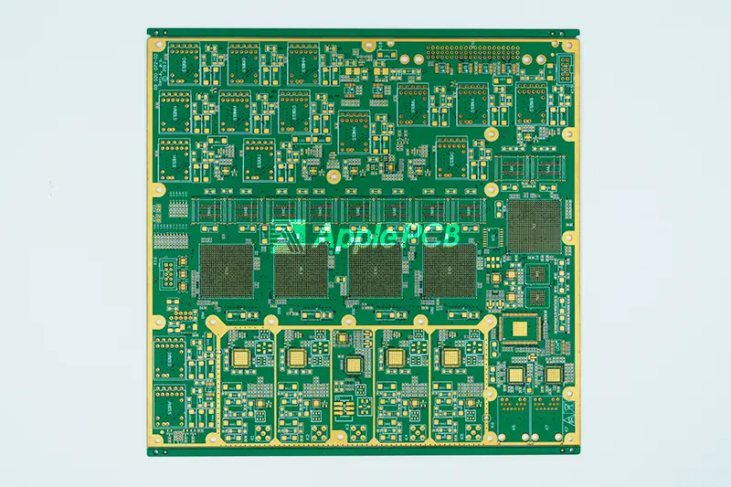
3.Signal Integrity and Impedance Control
For high-speed or RF designs, trace width is about more than just carrying current — it’s about signal quality. If the impedance along the signal path isn’t consistent, reflections, distortion, or delay can occur. Impedance depends on the trace width, spacing, copper thickness, and the dielectric layer’s thickness. Narrower traces raise impedance; wider ones lower it.
That’s why in high-speed circuits like USB, HDMI, or RF modules, designers must tightly control both trace width and spacing. Even a tiny deviation of a few mils can throw off the signal, especially at high frequencies.
3.Trace Shape and Reflection
Signal reflections often happen at sharp corners or abrupt shape changes in the routing. A 90-degree bend, for instance, changes the trace width and the local impedance, causing part of the signal to reflect back to the source. The result can be interference or data errors.
To prevent this, experienced PCB designers avoid sharp turns. They use 45-degree bends or smooth arcs instead. This keeps the signal flow steady and reduces impedance variations. Small design choices like these make a big difference in maintaining signal integrity in high-speed circuits.
4.Copper Thickness and Its Impact on PCB Design
No matter how advanced a design is, it still has to be manufacturable. Every PCB process has limits — the board material, number of layers, and copper thickness all determine how fine the traces and spacing can be. As the copper layer gets thicker, etching becomes harder to control, and issues like rough edges or trace shifting are more likely to appear. Ignoring these limits can easily lead to shorts, opens, or poor etching quality.
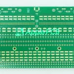
●Standard Copper (0.5–1 oz/ft², about 17.5–35 μm)
This is the most common option for signal and control boards. Standard manufacturing processes can reliably produce 5-mil trace widths and spacing.
●Heavy Copper (2–20 oz/ft², about 70–711 μm)
Used in high-current circuits, power modules, and other high-power applications. These heavy copper PCBs require much higher etching precision, so we recommend keeping trace width and spacing at 8 mils or greater.
●Extreme Thick Copper (24–200 oz/ft², about 850–7112 μm)
Designed for very high current or harsh industrial conditions. Such boards push the limits of fabrication equipment and often need custom processes, which naturally increase production time and cost.
While thicker copper improves conductivity and current-carrying capability, it also makes fabrication more challenging and expensive. That’s why early communication with your PCB manufacturer is essential. Confirming process limits up front helps balance performance, cost, and manufacturability.
How PCB Trace Design Affects Manufacturing Costs
In PCB production, trace width not only impacts performance but also directly determines manufacturing costs. As designs enter precision or high-density stages, manufacturing complexity increases significantly, naturally driving up costs. The following scenarios typically elevate PCB pricing:
●Traces Too Fine (<5mil)
Ultra-fine traces demand higher precision in exposure, etching, and inspection equipment. Production tolerances must be stricter; excessive deviations easily cause breaks or shorts, increasing scrap rates.
●Trace Spacing < 5mil
Smaller spacing between traces requires tighter etching control and higher cleanliness standards. It increases the risk of bridging or copper residue, necessitating additional inspection steps to ensure safe distances.
●Microvia Diameter <8mil
Small vias require laser drilling or high-precision mechanical drills. Such process equipment is costly and extends processing time.
●Non-Standard Copper Thickness< or > 1 oz/ft²
Thinner copper layers increase fracture risk, while thicker layers exponentially increase etching difficulty. Both scenarios demand specialized processes—such as multiple etch passes or plating compensation—thereby raising overall manufacturing costs.
●Differential Pairs and Controlled Impedance Design
These designs demand high consistency in trace width, spacing, and length. To guarantee impedance accuracy, manufacturers must repeatedly adjust and test board materials, copper thickness, and dielectric parameters, significantly increasing manufacturing complexity.
Simply put, designs pushing closer to manufacturing limits incur higher costs.
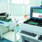
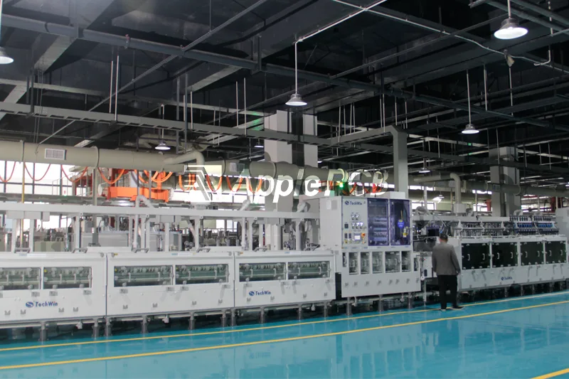
Utilizing Professional PCB Manufacturing and Assembly Services
In PCB layout design, relying solely on personal experience often makes it difficult to balance performance, cost, and manufacturability. Optimizing a circuit board requires not only solid expertise but also comprehensive process considerations and strict quality control. Choosing the right manufacturing partner is a crucial step in ensuring your design comes to life.
In complex circuit designs, errors often lurk in the details. Rather than reworking issues later, collaborate with an experienced manufacturer during the design phase. ApplePCB brings years of expertise in high-precision PCB manufacturing and assembly. Our engineering team employs Design Rule Checks (DRC) and Design for Manufacturability (DFM) analysis to help you identify potential problems and optimize layouts.
Whether you require multilayer PCB, thick copper power PCB, or other custom solutions, ApplePCB delivers a one-stop solution from design and prototyping to mass production. We make your designs more reliable and your delivery more efficient.