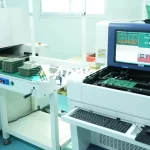
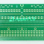
In PCB manufacturing, if circuit design serves as the blueprint that gives a board its function, then PCB etching is the precise "sculpting" process that brings that design to life. Etching is not just a simple corrosion; it is a critical process that carefully removes excess copper from the copper-clad board, turning the design into a fully functional and reliable circuit.
There are two main etching techniques used in modern PCB manufacturing: wet etching and dry etching. What are the differences between these methods, and how do you choose the best one for your project? In this article, we will explore the principles, characteristics, and ideal use cases for each method, helping you select the right technique for your product from the many available technical options.
PCB Wet Etching
Wet etching is the most widely used traditional process in PCB manufacturing. Its core principle involves utilizing acidic or alkaline chemical solutions to react with copper foil through redox reactions, selectively dissolving and removing exposed copper areas not protected by the resist layer to ultimately form the desired circuit pattern.
Based on the interaction method between the etchant and the board substrate, wet etching can be primarily categorized into two types:
- Immersion Etching
This method involves submerging the entire circuit board directly into a tank containing the chemical etching solution, completing the reaction through continuous immersion. This approach features simple equipment and high production capacity, making it suitable for mass production.
- Spray Etching
In this process, the etchant is uniformly sprayed onto the board surface via high-pressure nozzles. Simultaneously, the boards are typically in motion (e.g., conveyed or rotated) and supported by liquid suction devices to ensure uniform solution exchange and etching efficiency.
PCB Dry Etching

Unlike wet etching, dry etching is an advanced process that removes material using plasma within a vacuum environment. Its core principle involves ionizing specific gases (such as fluorine-based or chlorine-based gases) into highly reactive plasma using radiofrequency power sources. Guided by an electric field, this plasma physically bombards and chemically reacts with the substrate surface, precisely stripping and evaporating unprotected copper atoms to achieve anisotropic etching.
The primary technical types of dry etching include:
- Ion Beam Etching (IBE)
Directly removes material through physical bombardment of the substrate surface by a high-energy argon ion beam. This method is relatively slow but exhibits excellent directionality, enabling nanometer-level etching precision. It is suitable for processing materials requiring extremely high precision.
- Inductively Coupled Plasma Reactive Ion Etching (ICP-RIE)
This is an enhanced version of RIE, incorporating an inductively coupled plasma source into the traditional RIE setup. This plasma is generated by an RF-driven magnetic field and integrated with the original system. The additional plasma source provides greater control over the parameters of the dry etching process.
- Reactive Ion Etching (RIE)
Reactive ion etching is a dry etching method that utilizes reactive ions for material removal. The workpiece is typically placed on a high-frequency electrode. The electric field generated by this electrode influences ion movement within the chamber, enabling control over the etching direction. This approach achieves highly anisotropic etching channels. By adjusting the chamber pressure, the mean free path of particles can be altered, making the etching more directional or more isotropic, resulting in varying degrees of channel morphology.
- Plasma Etching
Characterized by forming nearly isotropic etch profiles, it is commonly used for uniform removal of entire thin film layers. This method relies primarily on the direct bombardment of plasma neutral particles to progressively remove material surfaces. Although often broadly categorized as dry etching, plasma etching can technically be regarded as a distinct form within dry etching processes.
PCB Wet Etching vs PCB Dry Etching
Wet etching processes can operate at atmospheric pressure, offer relatively fast etching speeds, and exhibit excellent material selectivity, making them suitable for processing a wide range of substrates. Additionally, such equipment is relatively easy to maintain, and the resulting surfaces are typically smooth and uniform. However, wet etching has limited capability when handling sub-micron details, making it difficult to achieve precise engraving on structures smaller than 1 µm. Due to the use of large quantities of chemical solutions, wastewater treatment poses significant challenges and may introduce risks of ionic contamination. Direct contact with chemical liquids and volatiles during operation can also lead to issues such as reduced adhesion between resistive components and the substrate.
Dry etching offers significant advantages in precision circuit processing, achieving uniform and precise etching at smaller feature sizes. It prevents lateral collapse during material removal, yielding narrow lines with sharp contours and minimal defects. However, compared to wet etching, dry processes demand higher equipment investment and require stringent process conditions with complex control systems. Furthermore, while plasma etching offers strong material adaptability, improper handling during processing may cause surface damage or safety hazards.
How to Select the Appropriate Etching Method?
1.Material Compatibility
Before determining the etching method, it is essential to understand the characteristics of the material being processed. Material type, film structure, and process requirements all influence the choice between plasma dry etching and liquid-based wet etching. Ideally, select the etching method that best enhances material performance and aligns with design specifications.
2.Etch Rate and Processing Efficiency
Different etching technologies exhibit varying speeds and precision. Dry etching achieves higher accuracy through process parameter tuning, making it suitable for projects demanding strict dimensional control. Wet etching offers simpler programming and operation with lower energy consumption, ideal for high-throughput production lines.
3.Feature Size and Profile Control Capability
Dry etching enables the formation of vertical sidewalls and high aspect ratio structures, offering superior control over feature dimensions. When evaluating options, clearly define the final pattern's line width, depth ratio, and sidewall morphology requirements before matching them with the appropriate process.
4.Environmental and Safety Impacts
Each etching method imposes distinct environmental and occupational safety requirements. Wet etching utilizes substantial chemical solutions, generating waste liquids requiring stringent treatment, though its overall environmental impact is relatively lower. Dry etching, relying on high-energy plasma systems, may produce gaseous emissions necessitating comprehensive safety precautions.
5.Cost and Equipment Complexity
Overall, wet etching is more cost-effective. Dry etching equipment is technologically advanced and complex, resulting in higher investment and maintenance costs. Wet etching equipment features simpler structures and lower operational difficulty, making overall costs more manageable.
Balancing investment against budget, production capacity, and manufacturing requirements enables enterprises to make more rational choices.
Final Thoughts
At ApplePCB, we deeply understand that “there is no single best process—only the most suitable solution.” With both mature wet etching production lines and advanced dry etching capabilities, we provide truly objective, professional process selection recommendations and one-stop manufacturing services tailored to your PCB design, performance requirements, and budget planning. Contact our engineering team today to obtain the optimal PCB etching solution for your project.