In the fast-paced world of electronics manufacturing, the focus is often on "smaller, thinner, and more precise, with Surface Mount Technology (SMT) seemingly taking over. However, when it comes to high-power components or mechanical interfaces, nothing beats the durability of pins that go through the board and are soldered securely on both sides. This strong, deep connection is why PCB through-hole technology remains essential in industries like aerospace, industrial power supplies, and high-end audio equipment.
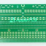
A PCB through hole is a channel created in a PCB using a mechanical drilling process. Electronic components with pins, like power resistors, large capacitors, or heavy connectors, are inserted into these holes. The components are then fixed in place by soldering on the back (or both sides) of the PCB.
What’s the Difference Between PTH and NPTH?
In PCB layout, holes play multiple roles, such as conducting signals, positioning components, managing heat, and dividing the board into sections. Based on whether the hole walls are metalized, PCB through holes are categorized into PTH and NPTH.
PTH (Plated Through Hole)
PTH is a hole that undergoes a metalization process, where a thin layer of copper is deposited on its walls. This process is used to create electrical connections between the different layers of a circuit board.
Key functions:
- Component soldering: PTH is central to through hole PCB assembly, used for inserting and soldering the pins of traditional through hole components (DIP).
- Via: Smaller PTHs are referred to as "vias," and they connect copper traces between multilayer PCBs, facilitating signal transmission across layers.
Design characteristics:
PTH typically includes an annular ring, with a copper layer on the pad tightly bonded to the hole walls, ensuring both electrical reliability and mechanical strength.
NPTH (Non-Plated Through Hole)
Unlike PTH, NPTH refers to holes that are not metalized, meaning they lack copper layers on their walls and do not conduct electricity.
Key functions:
- Mechanical positioning and securing: NPTH is mainly used for mounting screws, locating pins, or routing holes. Since these holes are non conductive, they help prevent accidental shorts between the circuit and mounting components like metal screws.
- Electrical isolation: In PCB design, NPTH serves as a physical barrier to ensure no signal interference occurs between the upper and lower layers of the board in specific regions.
Design features:
Typically, NPTH does not have an annular ring to maintain insulation. However, in certain applications, such as shielding or grounding, an annular ring may be added around the NPTH.
Advantages of PCB Through Hole
Let’s explore the core advantages of through-hole PCB assembly from two key aspects: design flexibility and manufacturing feasibility.
Through Hole PCB Design
- Mechanical strength: Unlike SMT components that are simply "mounted" on the surface pads, through-hole components have pins that go through the board and are fully surrounded by solder. This "through" connection provides far better pull and impact resistance than surface-mount technology. For components that frequently endure physical stress, such as switches, battery holders, and connectors, PTH is the only option to ensure the structure remains intact.
- High-power applications: High current circuits require larger electrical contact areas. Through hole connections offer a more reliable conductive path and can better support heavy components like heat sinks. Many high voltage, high power devices (such as large transformers) are still not available in equivalent SMT versions due to their weight and heat dissipation needs.
Through Hole PCB Manufacturing
- Prototype development and manual soldering: In the early stages of development or small-scale production, knowing how to solder through-hole PCBs is a crucial skill for technicians. In contrast to the high equipment demands of SMT, through hole components are much easier to solder by hand, which significantly lowers the barriers to creating prototypes.
- Serviceability: When a PCB needs component replacement or design modifications, removing and re-soldering through hole components is much easier and less likely to damage delicate pads compared to surface mounted components.
Why Has SMT Gradually Replaced Most of PTH?
Although Through-Hole PCB Assembly is highly reliable, it has some clear limitations when it comes to the modern electronics industry's focus on "high performance and miniaturization."
As a PCB manufacturer with 16 years of experience, we believe that when deciding whether to use THT (Through Hole Technology), it's crucial to objectively assess its challenges in production efficiency and design density. Below are some of the key drawbacks of through hole technology compared to SMT.
Disadvantages of PCB Through Hole
- Low space utilization: Each through-hole component must pass through all circuit layers, meaning that drilling occupies space across all layers, making it difficult to achieve high-density routing on multi-layer boards. On the other hand, SMT only uses the surface layer, allowing more components to be placed on the back.
- Dependence on manual labor: While we provide advanced through-hole PCB assembly services, it's important to acknowledge that although wave soldering handles mass soldering, the "insertion" step still can't be fully automated, especially when dealing with complex or irregular components. Technicians must manually align the component pins with the holes, bend them, and solder. As a result, the likelihood of human error (such as cold solder joints or solder bridges) is higher compared to fully automated SMT production lines.
- Component damage: The through-hole PCB assembly process exposes components to more challenging physical and thermal conditions. Pin insertion and bending can lead to pin breakage or ceramic package cracking, particularly with precision components. Additionally, unlike SMT's reflow soldering, manual or wave soldering generates more concentrated heat. If temperature control isn't precise, the sudden high temperatures can damage the internal structure of components, increasing defect rates and reducing overall production yield.
Why Is Professional Through-Hole Assembly Service Necessary?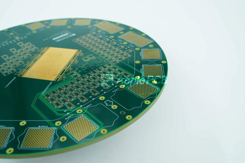
In real-world electronics manufacturing, Through-Hole PCB and SMT are not mutually exclusive. In fact, most modern high-tech electronic devices use Hybrid Assembly.
Though through-hole assembly might seem like a traditional process, it actually demands high technical expertise. A professional through-hole PCB assembly service goes beyond just soldering components onto the board; its real value lies in:
- Thermal management: How can temperature be precisely controlled during wave soldering to ensure the solder flows perfectly without causing heat damage to delicate components?
- DFM support: A skilled manufacturing team will review the design before assembly, checking the width of the pad ring (Annular Ring) and hole diameter tolerances. Even a small design tweak can significantly enhance the long-term reliability of plated through-hole PCBs and reduce defect rates.
- Consistency in hybrid assembly: It's important to ensure that the SMT reflow soldering process integrates seamlessly with the through hole wave soldering (or selective soldering) process, avoiding any secondary heat exposure that could affect already mounted components.
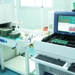
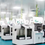
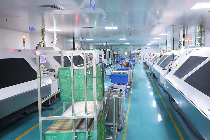
ApplePCB offers one-stop PCB services, from design review to through hole PCB Manufacturing. Feel free to send your Gerber files at any time.