In the PCB manufacturing industry, you’ve probably heard the term "AOI" quite often. At first, you might think it’s just another complex technical term. But in reality, Automated Optical Inspection (AOI) is like a vigilant set of electronic eyes on the production line, quickly spotting potential issues with the circuit boards. This helps minimize risks before the product even reaches the customer.
What is AOI?
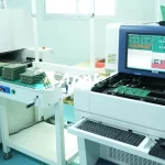
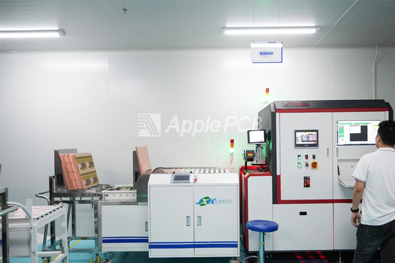
Automated Optical Inspection is a vision-based quality control method designed to detect potential issues during the PCB manufacturing and assembly process. Using high-resolution cameras, it scans the circuit boards to identify surface defects such as stains, scratches, open circuits, shorts, and problems like missing, incorrectly placed, or misaligned components.
Throughout production, the circuit boards typically go through Automated Optical Inspection at key stages: after the bare board etching, after the solder paste printing (often alongside SPI), and before and after the SMT and reflow soldering. The system takes multiple images and creates a reference standard, or "golden board," for a fully qualified circuit board. In subsequent batch production, Automated Optical Inspection compares new boards to this standard and automatically flags any potential defects for technicians to review and correct
Why is AOI Important for PCBs?
Ensuring Quality
AOI automatically inspects circuit boards during production, identifying defects like missing components, soldering issues, or circuit problems. This guarantees that every PCB you receive has been thoroughly checked, improving reliability and reducing the likelihood of issues.
Reducing Risk and Costs
Automated Optical Inspection helps manufacturers quickly identify defects caused by process issues and track patterns of defects, allowing them to optimize processes before problems worsen. Research shows that catching defects early in the production process can reduce repair costs by as much as 90%. However, if defects make it to the customer, the cost could increase by up to a thousand times.
Managing Complex PCB Designs
Inspecting high-density, multi-component PCBs manually is challenging. AOI, however, provides far greater accuracy than the human eye. Even when a board contains hundreds of components, Automated Optical Inspection can quickly detect missing or misaligned parts.
Flexibility to Meet Your Needs
Although AOI is an automated inspection process, the detection parameters can be adjusted to suit different designs. It can easily modify detection standards or adapt to new designs, keeping the production line running smoothly and efficiently.
What Issues Can AOI Detect?
Automated Optical Inspection systems are capable of detecting various types of defects. Below is a breakdown of some common issues to help you better understand AOI's detection capabilities:
| Category | Common Defects | Description |
| Soldering Defects | Insufficient solder, excess solder, solder bridges, insufficient solder paste, misaligned solder paste, lack of fill testing | Poor soldering can cause open circuits, shorts, or weak connections. |
| Component Defects | Incorrect components, missing components, misaligned components, incorrect polarity, flipped components, tombstoning, skewed components, lead lifting, severely damaged components | These issues relate to component placement and can negatively impact the board's functionality and reliability. |
| Structural/Geometric Defects | Height defects, volume defects, area defects | Problems with the 3D shape of solder joints, which could lead to cold soldering or insufficient strength. |
| Electrical/Design Rule Defects | Short circuits, violations of line width and spacing, excessive copper, missing pads, cutting issues, via fractures, improper component installation | These defects are related to the PCB design and manufacturing process, affecting both electrical performance and assembly accuracy. |
Differences Between 2D AOI and 3D AOI
In PCB inspection, AOI is mainly divided into two types: 2D and 3D. The core difference between them lies in how they "look at" the board, which ultimately determines their strengths and limitations.
Image Capture Method
2D AOI captures a 2D image of the circuit board from a single angle, similar to taking a photo. In contrast, 3D AOI captures images from multiple angles and creates a 3D model of the board.
Depth Perception
Since 2D AOI only views the board from a flat, 2D perspective, it may miss defects in more complex solder joints or stacked components. 3D AOI, however, incorporates depth information, enabling it to detect issues that a single-angle view might overlook. This makes it ideal for high-density designs.
Inspection Speed
2D AOI is faster, making it well-suited for high-volume, fast-paced production lines. 3D AOI takes a bit more time but delivers more detailed and thorough inspections.
Accuracy
When it comes to precision, 3D AOI is the superior option, offering a more complete view and better defect detection. While 2D AOI is sufficient for most routine inspections, it may fall short in high-precision applications.
Cost Investment
2D AOI equipment is more affordable, making it a better fit for cost-sensitive production environments. 3D AOI, which involves more complex hardware and software, requires a higher upfront investment, but it provides superior detection quality.
The Relationship Between AOI, AXI, and ICT
In PCB quality control, AOI, AXI and ICT work together as complementary technologies. Each method specializes in detecting different types of defects, helping to cover a wide range of potential issues in PCB production.
●AOI: This is primarily used for detecting surface defects such as soldering issues, misaligned components, missing parts, and solder bridges. These problems are usually identified after SMT placement and reflow soldering and are among the most common defects found in PCBs.
●AXI: AXI is focused on detecting hidden defects within the PCB or those that cannot be seen from the surface, such as solder joints in BGA (Ball Grid Array) packages. Since these joints are not visible through standard inspection, AXI uses X-ray technology to inspect them by penetrating through the board.
●ICT: ICT is used to verify the PCB’s electrical performance, such as detecting open or short circuits. It is typically performed after the PCB is fully assembled to ensure that the electrical connections are functioning correctly.
To achieve the highest detection efficiency and accuracy, modern PCB production often employs a layered inspection strategy: SPI (Solder Paste Inspection) → AOI → AXI/ICT. This approach progressively improves the first pass yield, ensuring that every PCB meets quality standards.
FAQ
Can AOI still detect defects effectively if my design is complex?
Yes, AOI is highly effective at spotting even the most subtle defects in complex designs. It can handle high-density circuit boards and intricate soldering with ease, using advanced image capture and analysis technology to detect issues that might be missed by the human eye.
Will using Automated Optical Inspection increase the cost of my PCBs?
While there may be a higher initial investment in AOI systems, the long-term savings are substantial. Automated Optical Inspection significantly reduces rework, repairs, and waste, ultimately saving you more by improving efficiency across production.
Can AOI ensure that my PCBs meet industry standards?
Yes, we follow industry standards such as IPC-A-610 closely and conduct inspections with AOI. The system evaluates PCBs based on different quality levels (Class 1/2/3), ensuring that your products meet both industry requirements and customer expectations.
Can AOI reduce the risk of PCB rework and damage?
Absolutely! Automated Optical Inspection is great at quickly identifying issues like poor soldering, missing components, or misalignment, preventing defective products from proceeding further down the line or being delivered to customers.
Can AOI’s inspection speed keep up with high-volume production?
Yes, AOI is designed for high-speed inspections and can easily handle large-scale production. It can quickly process a large number of PCBs and deliver precise results in a short amount of time.