A test point on a PCB is an exposed metal contact on the outer layer, connected to a network within the circuit. It provides a convenient spot for measuring or probing signals, power, or connections during both production and after the product is made. In this article, we’ll discuss why test points are essential, the different types and practices of using them, and some common challenges encountered during the manufacturing process.
Why Are PCB Test Points Necessary?
Incorporating test points into your PCB design is a smart decision, as these small contact points can help with several critical tasks.
Ensuring Proper Circuit Functionality
They allow for quick checks to confirm whether the key power, ground, and signal networks are properly connected and meet the required design specifications. This process is important during every stage of production, both before and after the PCB is assembled.
Speeding Up Debugging and Repairs
If a board malfunctions, engineers can easily probe the test points to pinpoint the issue, avoiding the need to desolder components or risk damaging the board.
Supporting Automated Testing in Mass Production
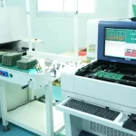
On production lines, they are crucial for automated testing methods like ICT or Flying Probe tests. These interfaces help ensure efficient and consistent testing of hundreds of boards, saving both time and money on each unit.
Reducing Costs and Risks
By catching issues early through test points, you can avoid costly repairs or returns after shipping, ultimately lowering the failure rate and reducing overall production costs.
Beneficial for Both Prototypes and Mass Production
Even in the early development phase, test points are valuable for verifying key design elements. In high-volume manufacturing, they play an important role in maintaining overall quality control and streamlining production processes.
Types of PCB Test Points
In the PCB manufacturing process, we generally use two main categories of test points.
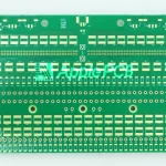
The first category is "Manufacturing Test Points," which are used by technicians with handheld instruments. These points are typically fitted with a small post to make it easier for probes to clamp onto. We also mark the test point's location and the corresponding network name on the silkscreen for easy identification.
The second category is "Assembly Test Points," designed for use with automated testing equipment. These test points are usually through-hole pins, vias, or small pads that work with the probes of automated machines.
In automated testing, there are three common methods:
1.Bare Board Testing: This test is performed before any components are installed, where the PCB’s copper traces and vias are inspected for open or short circuits. The main goal is to verify that all electrical networks on the board are properly connected.
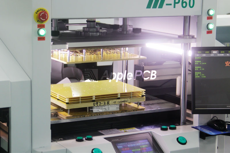
2.In-Circuit Testing: After the board is assembled, technicians place it in a fixture with probes. The probes check the test points to confirm that each component is installed correctly, oriented properly, and soldered well.
3.Flying Probe Testing: This test is also done after assembly, but instead of fixed probes, two to six movable probes are used to make contact with the test points from various angles, allowing for the measurement of signals and voltages.
| Item | In Circuit Testing | Flying Probe Testing |
| Fixture / Setup | Requires a custom “bed-of-nails” fixture with spring-loaded pins contacting many test points simultaneously. | No dedicated fixture needed. Uses movable probes that access test points via software control. |
| Up-front cost & lead time | High initial investment; longer setup time for fixture design and build. | Low initial cost; faster set-up since no fixture manufacturing required. |
| Test cycle speed / per-unit cost | Very fast per board once setup; lower cost per unit in high volumes. | Slower per board; higher cost per unit in high-volume runs. |
| Coverage & capability | Very comprehensive: checks opens, shorts, component values, direction, solder joints; ideal for mature designs. | Flexible and good for many tests; less optimal for extremely high volume or designs requiring maximum coverage. |
| Best use scenario | High volume production with stable and mature design; cost efficiency is key. | Prototypes, low/medium volume runs, design still evolving, high flexibility needed. |
| Limitations | High upfront cost, less suited for small batches or rapidly changing designs. | Slower testing, higher cost per board in large scale, coverage may be less ideal in some cases. |
Best Practices for Test Points Across Different PCB Types
Rigid PCB
- For mass production, it's advisable to use ICT-compatible test pads in rigid PCB.
- Make sure the spacing between test points is consistent across the automated testing fixtures.
- It’s a good idea to design the board following a standard "bed of nails" test pattern for smoother batch testing.
Flex / Rigid-Flex PCB
- Avoid placing test points in areas that experience bending or movement to minimize mechanical stress.
- Reinforce the pads at probe contact points to improve accessibility.
- If probes cannot easily access flexible areas, consider using specialized connectors instead of relying on traditional probe access methods.
High-Frequency / High-Speed PCB
- Place test points on controlled impedance traces to minimize disruption to signal integrity.
- Use vias instead of large pads to maintain better signal characteristics.
- For RF or high-speed modules, shield the test points to avoid crosstalk and signal degradation.
Common Issues & Troubleshooting for Test Point Implementation
- Small test point pads: If the probe contact area is too small, it will reduce reliability. Ensure the pads are properly sized.
- High-density PCBs: When the layout is dense and probes are difficult to insert, consider using specialized test fixtures or edge connectors.
- Solder mask: If the test points are covered by the solder mask, probes won’t make contact. Ensure test points are fully exposed.
- Insufficient test coverage: If key networks don’t have accessible test points, fault detection will be more difficult.
- Probes affected by mechanical stress: If probes are repeatedly contacted with high pressure, use durable hard gold plating to withstand wear.
- Missing ground test points: Without ground reference points when measuring signals or voltage, results will be inaccurate. Ensure ground test points are included.
Final Thoughts
Test points play a small but vital role in PCB design. Proper planning of test points can improve manufacturing efficiency, reduce rework rates, and accelerate debugging processes. Designers, manufacturers, and customers should consider DFT (Design for Test) and test point layout from the very beginning of the project. As automation and high-speed circuits continue to develop, the design of test points will evolve (for example, with hidden test points or wireless test interfaces)—but the core principles will stay the same: they must be measurable, accessible, and reliable.