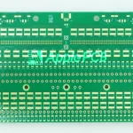
Most designers start their career with the 2-layer PCB. It isn't complicated. Think of it as the "Hello World" of hardware: simple, logical, and fast. While it lacks the dense stack-up of a multilayer pcb, this double-layer design still forms the spine of many great products.
Don't let the simplicity fool you, though. How does a designer optimize a 2-layer PCB ground plane in such tight space? How do they dodge EMI? Master the logic of this board, and you get an entry ticket to complex system design.
Understanding the 2-Layer PCB Stack-up
A 2-layer board uses a top and bottom conductive layer separated by an insulator. Let’s look at what's inside.
- Copper Layer: Each side uses copper foil. Vias—small copper-plated holes—connect the two sides. This lets the signal move freely from top to bottom.
- Signal Layer: Both copper sides hold the pad and trace. Each one handles signal duty.
- Power Layer: This layer pushes power across the board. It also acts as the return path for a ground signal to keep power steady. On a 2-layer PCB, designers usually use a large copper pour or grid for power and ground.
- Dielectric Layer(Insulation): A thin dielectric material—the core or prepreg—sits between the copper. It does two things. First, it stops a short circuit between the top and bottom. Second, it provides a strong base so the board stays stiff.
- Solder Mask and Silkscreen: The outer layer uses solder mask ink (usually green). It stops a short during soldering and holds printed info like:
Through this layered design, the 2-layer PCB achieves four core functions—signal transmission, power distribution, electrical isolation, and information identification—with the simplest structure, making it the preferred solution for most low-cost electronic products.
2-Layer PCB Design Rule
The 2-layer PCB might not handle a high-end FPGA or a complex BGA package, but it's still the go-to for consumer gear, IoT device, and microcontroller.
1.Watch Trace Width and Drill Size
Don't shrink a dimension just to chase extreme density. Keep the signal trace at 6 mil—it's enough for 1A of DC. For a power line, go up to 20 mil to support a 3A load. Pair this with a 13 mil drill hole. Why? Because it hits the sweet spot for performance without adding to the fab bill.
2.Fix Signal and Return Path
Good layer assignment solves half the noise problem. Usually, the top layer acts as the main home for power and signal. The bottom layer handles the component route and ground loop. The real trick? Keep a solid ground plane right under the signal trace. This ensures the shortest return path and keeps impedance low.
3.Cut Congestion With Better Layout
Messy routing causes crosstalk. When a designer places a component, they should plan the signal flow early to stop a trace from crossing another. Add extra space between signal lines, especially on a long parallel run. This stops interference caused by shifts in characteristic impedance.
4.Keep the Path Short
Every design choice should focus on low impedance. Keep every trace as short as possible. This ensures mutual inductance in the return path stays low. If a route has to be long, use a return strap to give the signal a clear way back.
5.Place Decoupling Capacitor Wisely
A decoupling capacitor must sit right against the IC power pin. To stop a current surge, use a capacitor with a voltage rating that is double the application voltage. A 22 uF MLCC is almost always a safe bet.
6.Control Connector Signal Return
Switching noise and ground bounce happen when too many signals share one return pin. If space allows, give every key digital signal its own return path. Don't let high-speed signals crowd a single pin. It’s the last line of defense for a steady system.
Common Myths About 2-Layer and 4-Layer PCBs
When picking a circuit board, many designers fall into a logical trap: "more layers mean more trouble." It's a mistake. A few common myths about the 2-layer PCB often push an engineer to make a bad call between performance and cost.
1.The Cost Myth
A new designer usually thinks a 4-layer board costs a fortune. Sure, if you do a quick-turn prototype in North America, you'll pay a premium for those extra steps. But look at the big picture. What happens if a 2-layer PCB fails an EMC test and you have to redo the whole project? That cost is way higher than starting with 4 layers. Plus, in the Chinese market, the price gap is shrinking fast. For a long-lead-time order, a 4-layer PCB might even have a better price.
2.The Performance Myth
Some people think a 2-layer PCB only works for a "slow signal." That isn't true. Shielding is harder, yes. But if a designer has enough space to put a solid ground plane on the back, the board can handle USB or 10/100 Ethernet just fine. Why? Because a designer can use a coplanar ground fill and bottom grounding to hit a precise, controlled impedance.
3.The RF Myth
This is like the performance myth. Even at a GHz frequency, a designer can route a signal with Coplanar Waveguide (CPW) tech. Think about it: even on a 6-layer board, an RF feedline works almost exactly like it does on 2 layers. The core logic for an antenna usually stays on the top and bottom anyway. If you get the via spacing right, 2 layers can do a lot in the RF world.
4.The Difficulty Myth
This is a classic gut-feeling error. Ask anyone who has worked on a 4-layer board, and they’ll tell you: it is much easier to layout than a 2-layer PCB. With two dedicated ground planes, you don't have to fight with complex "cross" routing to stop crosstalk. Power distribution is easy, too. You can use a large copper pour to connect a part instead of trying to snake a trace through a crowded signal layer.
Choosing a 2-Layer PCB Manufacturer
Picking a maker is the final hurdle. Even a simple 2-layer PCB needs a good factory, or your scrap rate will go through the roof. Before you buy, check the 2-Layer PCB Manufacturer's capability. That's the only way to ensure the project actually works.
ApplePCB’s Manufacturing Capabilities
| Item | Process Capability |
| Layer Count | 1-36 Layers |
| Board Thickness | 0.2-8mm, Tolerance ±5% |
| Maximum PCB Size | 500x1500mm |
| Material Type | FR-4, PTFE, ROGERS, ARLON, etc. |
| Copper Thickness | Range from 1/2 oz to 20 oz |
| Advanced Drilling | Machine Drill: 0.15mm-6.4mm |
| Laser Drill: 0.075mm-0.2mm | |
| Surface Finishing | HASL, LF HASL, ENIG, Immersion Tin/Silver/Gold, OSP, ETC. |
| Warp | Conventional: 0.75%;Limit:0.5%;Max:2.0%. |
| Impedance Control | ±7% |
| Testing Methods | AOI |
| Flying Probe | |
| In-Circuit | |
| X-Ray Inspection | |
| Functional Testing | |
| Certifications | IATF 16949:2016 |
| ISO 9001:2015 | |
| ISO 14001:2015 | |
| ISO 13485:2016 | |
| UL |
Ready to Start Your Next Project?
In a crowded market, ApplePCB keeps human error to a minimum with a fully automated production line. Upload a Gerber file now and get an instant quote from ApplePCB.