For a hardware engineer, a 6-layer PCB is almost the perfect fix for high-speed signal issues. Compared to a 4-layer design, the two extra internal layers act as dedicated ground and power planes. This setup provides a clean signal reference plane, killing troublesome crosstalk and electromagnetic interference at the source.
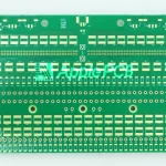
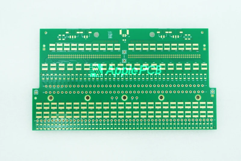
Look at it from the factory floor, though, and the story changes. Upgrading a design from a 4-layer to a 6-layer PCB is never as simple as dropping in two more sheets of copper foil. For the fabrication house, it means the complexity of the lamination process doubles overnight. Why does this transition change the manufacturing game? Let's look at a 6-layer PCB straight from the production floor.
Comparing 4-Layer and 6-Layer Stackups
From a structural standpoint, a standard 4-layer PCB features just two outer routing layers and two internal planes—typically dedicated to ground and power. A 6-layer PCB takes this foundation and adds two extra internal layers, which engineers use for signal routing or high-density shielding. Why make the switch? Because those extra layers give high-speed signals a continuous, clean return path. In fact, switching to a 6-layer layout can slash interlayer crosstalk by as much as 60%.
From a production viewpoint, a 4-layer PCB keeps initial fabrication costs low. However, if a project involves mixed-signal environments like combined digital-and-analog or RF routing, a 4-layer stackup raises the risk of EMI failure exponentially. Stick with a cost-effective 4-layer PCB if the project only handles basic digital logic or low-speed control. But the moment a design demands strict mixed-signal isolation, or a core chip requires a tight, continuous return path, an upgrade to a 6-layer stackup becomes essential.
Standard 6-Layer PCB Stackup Design
A stackup configuration details how a factory arranges 6 layers of copper foil and insulating dielectric material in a three-dimensional space. This layout acts as the physical backbone for a board's electrical performance, signal integrity (SI), and electromagnetic compatibility (EMC). The choice of stackup directly dictates impedance control accuracy, EMI shielding performance, crosstalk suppression, and long-term manufacturing reliability.
On the factory floor, production lines run three classic stackup configurations most often. Let's look at the first golden option.
Option 1: The Universal Balanced Stackup
This setup stands as the most common 6-layer configuration in modern electronics. It strikes an ideal commercial balance between signal routing freedom and power integrity.
Layer 1 (Top Signal): The primary signal routing layer where most core components live. It handles high-speed traces, critical control paths, and surface-mount device (SMD) pads.
Layer 2 (Ground Plane): A solid, unbroken ground reference. Its main job is to provide an immediate, continuous return path for Layer 1 signals. This layer serves as a clean reference for controlled impedance while shielding against EMI and cutting top-layer radiation.
Layer 3 (Internal Signal 1): A dedicated inner channel for high-speed traces, critical differential pairs, or sensitive analog paths. Sandwiched between Layer 2 (Ground) and Layer 5 (Power), it gains excellent physical noise protection.
Layer 4 (Internal Signal 2): An extra internal pathway for dense layouts, often used for general digital lines or mixed-signal routing. To stop interlayer crosstalk completely, fabrication guidelines recommend running these traces orthogonal—perpendicular—to Layer 3.
Layer 5 (Power Plane): A low-impedance power distribution layer delivering clean voltage across the board. For multi-rail designs, you can split this plane into distinct voltage zones like 3.3V, 5V, or 12V. It also acts as the signal return reference for Layer 6.
Layer 6 (Bottom Signal): The secondary routing layer on the back side. Use this to expand routing space when the top layer becomes crowded or when using double-sided SMT assembly.
Why does this specific layout remain an industry favorite? Because the proximity of Layer 2 (Ground) and Layer 5 (Power) creates strong inter-plane decoupling capacitance. This built-in capacitance clamps down on high-frequency switching noise at the source, keeping the power delivery network highly stable.
Option 2: High-Speed Digital Stackup (Dual Ground Planes)
When a hardware project operates in the ultra-high frequency domain—handling strict differential pairs like USB 3.0, HDMI, or PCIe—or when a product must pass brutal industry EMI certification benchmarks, a dual ground plane stackup is the superior choice.
Layer 1: Top Signal
Layer 2: GND Plane
Layer 3: High-Speed Signal
Layer 4: High-Speed Signal
Layer 5: GND Plane
Layer 6: Bottom Signal
By dropping two complete, unbroken ground planes into the center core (Layer 2 and Layer 5), this layout creates an ideal closed-loop reference environment for internal high-speed traces and differential pairs. Think about it: when high-frequency silicon switches states at nanosecond speeds, this dual-shield setup blocks electromagnetic noise completely and chokes out ground bounce at the physical limit.
Option 3: Mixed-Signal Isolation Stackup (Analog/Digital Separation)
Managing a mixed-signal board means fighting digital noise pollution. If a design places a weak, sensitive analog path (like a sensor front-end or audio amplifier) right next to a noisy digital core (like an MCU or FPGA), the layout demands physical isolation. This stackup design fixes that issue.
Layer 1: Top Signal
Layer 2: Ground Plane (Features a strict physical split between Analog GND and Digital GND)
Layer 3: Digital Signal
Layer 4: Analog Signal
Layer 5: Power Plane (Features separate Analog and Digital power rails)
Layer 6: Bottom Signal
Why does this arrangement work? Because it enforces total isolation by forcing signals into separate layers. Layer 3 belongs exclusively to high-noise digital routing, while Layer 4 remains dedicated to clean analog lines. On the manufacturing line, the factory mirrors this split by precision-etching distinct digital and analog zones right into the reference planes (Layer 2 and Layer 5), cutting off crosstalk at the structural level.
Understanding Cost Drivers in 6-Layer PCB Fabrication

While a 6-layer PCB involves a more intricate manufacturing process than a 4-layer alternative, you do not have to break the bank to build one. By aligning your design choices with the operational logic of the factory floor, you can significantly lower production costs without compromising hardware performance.
1.Material Selection
When configuring your stackup, always aim for the most common materials running on the factory line. The golden baseline for a cost-effective 6-layer board includes:
Overall Board Thickness: 1.6 mm
Outer Copper Weight: 1 oz
Substrate Material: Standard FR-4
Solder Mask: Green
Surface Finish: HASL
Fabrication houses run these exact specifications every single day. If you stray into non-standard territory—such as a 2.0 mm thickness, black solder mask, or a premium ENIG (immersion gold) finish—your board can no longer be panelized alongside other client orders. The factory must set up a dedicated production run just for you, which causes raw material costs and minimum order quantities (MOQs) to surge immediately.
2.Via Architecture
During dense layouts, it is tempting to use advanced HDI features like blind or buried vias to make routing easier. On the factory floor, however, blind and buried vias completely rewrite the production sequence.
Each set of microvias requires an extra lamination cycle, specialized laser drilling, and independent copper plating/hole-filling steps. This added complexity doubles lead times, increases yield risks, and drives manufacturing costs up exponentially. Unless you are packing circuitry into an ultra-compact wearable or an optical transceiver where every micrometer counts, stick to a standard through-hole architecture.
3.Order Consolidation
PCB manufacturing carries heavy upfront, fixed tooling costs. Every new run absorbs engineering time for DFM verification, photo-tooling film creation, and flying probe test programming.
If you bundle multiple small, scattered prototype runs from across your organization into a single consolidated batch, or if you release your high-volume production demand immediately following a successful prototype sign-off, you change the economics of the run. Amortizing these fixed tooling charges across a larger unit volume causes the piece price of each board to drop dramatically.
4.Lead Times
Unless a project is facing a catastrophic timeline failure, always schedule your production around the factory’s standard lead time. Standard scheduling keeps the facility running at its most efficient, predictable rhythm. Opting for a 24-hour or 48-hour quick-turn run means you are paying a heavy premium to cut the line, a fee structured to offset the idle capacity and tool-swapping penalties your disruption causes on the line.
5.Early DFM Reviews
Do not treat a manufacturing handoff as a final, transactional step. Instead of sending over completely locked Gerber files on the day of production, engage with your manufacturer's engineering team early during the layout phase for an in-depth Design for Manufacturability (DFM) assessment.
An experienced CAM engineer can spot opportunities from a fabrication perspective that a design tool might miss. They can identify trace tolerances that can be safely widened or point out specialized processes that can be swapped for standard methods, giving you a chance to strip out unnecessary production costs before a single layer is pressed.
Ready to Launch Your Next 6-layer PCB Design?
Get in touch with ApplePCB today. Upload your design files directly to our secure online portal for immediate pricing, or request a comprehensive DFM evaluation and engineering consultation. Our veteran technical support team is standing by to assist you.